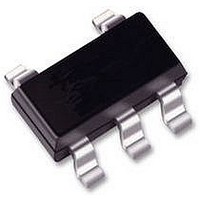
74LVC1G66GW NXP Semiconductors, 74LVC1G66GW Datasheet - Page 14

74LVC1G66GW
Manufacturer Part Number
74LVC1G66GW
Description
IC, LOGIC, 74LVC1G, SWITCH, UMT5
Manufacturer
NXP Semiconductors
Datasheet
1.74LVC1G66GW.pdf
(25 pages)
Specifications of 74LVC1G66GW
Analogue Switch Type
Bilateral Switch
No. Of Channels
1
Bandwidth
440MHz
Supply Voltage Range
1.65V To 5.5V
Operating Temperature Range
-40°C To +125°C
Analogue Switch Case Style
TSSOP
No. Of
RoHS Compliant
On State Resistance Max
23ohm
Rohs Compliant
Yes
Available stocks
Company
Part Number
Manufacturer
Quantity
Price
Company:
Part Number:
74LVC1G66GW
Manufacturer:
NXP
Quantity:
33 000
Part Number:
74LVC1G66GW
Manufacturer:
NXP/恩智浦
Quantity:
20 000
NXP Semiconductors
Table 12.
At recommended operating conditions; voltages are referenced to GND (ground = 0 V); T
74LVC1G66
Product data sheet
Symbol
Q
Fig 19. Test circuit for measuring total harmonic distortion
Fig 20. Test circuit for measuring the frequency response when switch is in ON-state
inj
Test conditions:
V
V
V
V
Adjust f
CC
CC
CC
CC
Additional dynamic characteristics
Parameter
charge injection
= 1.65 V: V
= 2.3 V: V
= 3 V: V
= 4.5 V: V
11.3 Test circuits
i
voltage to obtain 0 dBm level at output. Increase f
i
= 2.5 V (p-p).
i
i
= 2 V (p-p).
= 4 V (p-p).
i
= 1.4 V (p-p).
f i
V
IH
V
IH
0.1 μF
f i
50 Ω
All information provided in this document is subject to legal disclaimers.
C
Conditions
f
i
L
= 1 MHz; R
V
V
V
V
V
= 0.1 nF; V
CC
CC
CC
CC
CC
600 Ω
Y/Z
Y/Z
E
…continued
= 1.8 V
= 2.5 V
= 3.3 V
= 4.5 V
= 5.5 V
E
Rev. 7 — 30 July 2010
V
L
CC
V
gen
= 1 MΩ; see
CC
= 0 V; R
i
frequency until dB meter reads −3 dB.
Z/Y
Z/Y
0.5V
0.5V
gen
Figure 23
CC
CC
R L
= 0 Ω;
R L
C L
C L
10 μF
001aam392
dB
D
001aam393
V
O
amb
V
Min
-
-
-
-
-
O
= 25
74LVC1G66
Typ
3.3
4.1
5.0
6.4
7.5
°
C.
© NXP B.V. 2010. All rights reserved.
Bilateral switch
Max
-
-
-
-
-
Unit
pC
pC
pC
pC
pC
14 of 25


