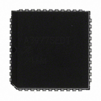
A3977SEDTR-T Allegro Microsystems Inc, A3977SEDTR-T Datasheet - Page 8

A3977SEDTR-T
Manufacturer Part Number
A3977SEDTR-T
Description
LEAD FREE A3977SEDTR
Manufacturer
Allegro Microsystems Inc
Datasheet
1.A3977SEDTR-T.pdf
(18 pages)
Specifications of A3977SEDTR-T
Rohs Compliant
YES
Applications
Stepper Motor Driver
Number Of Outputs
1
Current - Output
±2.5A
Voltage - Load
8 V ~ 35 V
Voltage - Supply
3 V ~ 5.5 V
Operating Temperature
-20°C ~ 85°C
Mounting Type
Surface Mount
Package / Case
44-LCC (J-Lead)
Motor Type
Stepper
No. Of Outputs
2
Output Current
2.5A
Output Voltage
35V
Supply Voltage Range
3V To 5.5V
Driver Case Style
LCC
No. Of Pins
44
Operating Temperature Range
-20°C To +85°C
Lead Free Status / RoHS Status
Lead free / RoHS Compliant
Other names
620-1146-2
A3977SEDTR-T
A3977SEDTR-T
Available stocks
Company
Part Number
Manufacturer
Quantity
Price
Company:
Part Number:
A3977SEDTR-T
Manufacturer:
ALLEGRO
Quantity:
1 500
Company:
Part Number:
A3977SEDTR-T
Manufacturer:
Allegro MicroSystems, LLC
Quantity:
10 000
A3977
Fixed Off-Time. The internal PWM current-control
circuitry uses a one shot to control the time the drivers
remain off. The one shot off-time, t
the selection of an external resistor (R
connected from the RC timing terminal to ground. The off-
time, over a range of values of C
R
RC Blanking. In addition to the fi xed off-time of the
PWM control circuit, the C
tor blanking time. This function blanks the output of the
current-sense comparator when the outputs are switched by
the internal current-control circuitry. The comparator out-
put is blanked to prevent false over-current detection due
to reverse recovery currents of the clamp diodes, and/or
switching transients related to the capacitance of the load.
The blank time t
Charge Pump. (CP
used to generate a gate supply greater than V
the source-side DMOS gates. A 0.22 μF ceramic capacitor
should be connected between CP
purposes. A 0.22 μF ceramic capacitor is required between
V
DMOS devices.
V
the sink-side DMOS outputs. The V
be decoupled with a 0.22 μF capacitor to ground. V
internally monitored and in the case of a fault condition,
the outputs of the device are disabled.
Enable Input (ENABLE). This active-low input enables
all of the DMOS outputs. When logic high the outputs are
disabled. Inputs to the translator (STEP, DIRECTION,
MS
input state.
T
REG
CP
= 12 kΩ to 100 kΩ is approximated by:
1
and V
, MS
. This internally generated voltage is used to operate
2
) are all active independent of the ENABLE
BB
to act as a reservoir to operate the high-side
BLANK
t
BLANK
1
can be approximated by:
and CP
t
off
= R
T
= 1400C
component sets the compara-
T
2
C
T
1
). The charge pump is
T
= 470 pF to 1500 pF and
and CP
off
REG
, is determined by
T
T
) and capacitor (C
Microstepping DMOS Driver with Translator
terminal should
Functional Description (cont’d)
2
for pumping
BB
to drive
REG
is
T
)
Shutdown. In the event of a fault (excessive junction
temperature, or low voltage on V
device are disabled until the fault condition is removed. At
power up, and in the event of low V
lockout (UVLO) circuit disables the drivers and resets the
translator to the HOME state.
Sleep Mode (SLEEP). An active-low control input used
to minimize power consumption when not in use. This
disables much of the internal circuitry including the output
DMOS, regulator, and charge pump. A logic high allows
normal operation and startup of the device in the home
position. When coming out of sleep mode, wait
1 ms before issuing a STEP command to allow the charge
pump (gate drive) to stabilize.
Percent Fast Decay Input (PFD). When a STEP input
signal commands a lower output current from the previous
step, it switches the output current decay to either slow-,
fast-, or mixed-decay depending on the voltage level at the
PFD input. If the voltage at the PFD input is greater than
0.6 V
on the PFD input is less than 0.21 V
mode is selected. Mixed decay is between these two levels.
This terminal should be decoupled with a 0.1 μF capacitor.
Mixed Decay Operation. If the voltage on the PFD in-
put is between 0.6V
ate in mixed-decay mode depending on the step sequence
(see fi gures). As the trip point is reached, the device will
go into fast-decay mode until the voltage on the RC termi-
nal decays to the voltage applied to the PFD terminal. The
time that the device operates in fast decay is approximated
by:
switch to slow-decay mode for the remainder of the fi xed
off-time period.
After this fast decay portion, t
DD
then slow-decay mode is selected. If the voltage
t
FD
= R
DD
T
and 0.21V
C
115 Northeast Cutoff
1.508.853.5000; www.allegromicro.com
Allegro MicroSystems, Inc.
Worcester, Massachusetts 01615-0036 U.S.A.
T
In (0.6V
CP
DD
FD
) the outputs of the
DD
DD
, the bridge will oper-
DD
, the device will
/V
, the undervoltage
then fast-decay
PFD
)
8


