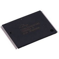
S29GL01GP11FFIR20 Spansion Inc., S29GL01GP11FFIR20 Datasheet - Page 49

S29GL01GP11FFIR20
Manufacturer Part Number
S29GL01GP11FFIR20
Description
Flash - NOR IC
Manufacturer
Spansion Inc.
Datasheet
1.S29GL01GP11FFIR20.pdf
(80 pages)
Specifications of S29GL01GP11FFIR20
Memory Size
1000Mbit
Memory Configuration
128K X 16
Ic Interface Type
CFI, Parallel
Access Time
110ns
Supply Voltage Range
3V To 3.6V
Memory Case Style
TSOP
No. Of Pins
64
Cell Type
NOR
Density
1Gb
Access Time (max)
110ns
Interface Type
Parallel
Boot Type
Not Required
Address Bus
27/26Bit
Operating Supply Voltage (typ)
3/3.3V
Operating Temp Range
-40C to 85C
Package Type
Fortified BGA
Sync/async
Asynchronous
Operating Temperature Classification
Industrial
Operating Supply Voltage (min)
3V
Operating Supply Voltage (max)
3.6V
Word Size
8/16Bit
Number Of Words
128M/64M
Supply Current
110mA
Mounting
Surface Mount
Pin Count
64
Lead Free Status / Rohs Status
Compliant
Available stocks
Company
Part Number
Manufacturer
Quantity
Price
Company:
Part Number:
S29GL01GP11FFIR20
Manufacturer:
SPANSION
Quantity:
1 000
9. Power Conservation Modes
9.1
9.2
9.3
9.4
November 17, 2010 S29GL-P_00_A13
8.6.3
8.6.4
Standby Mode
Automatic Sleep Mode
Hardware RESET# Input Operation
Output Disable (OE#)
Write Pulse “Glitch Protection”
Power-Up Write Inhibit
Noise pulses of less than 5 ns (typical) on OE#, CE# or WE# do not initiate a write cycle.
If WE# = CE# = RESET# = V
rising edge of WE#. The internal state machine is automatically reset to the read mode on power-up.
When the system is not reading or writing to the device, it can place the device in the standby mode. In this
mode, current consumption is greatly reduced, and the outputs are placed in the high impedance state,
independent of the OE# input. The device enters the CMOS standby mode when the CE# and RESET#
inputs are both held at V
is ready to read data. If the device is deselected during erasure or programming, the device draws active
current until the operation is completed. I
specification
The automatic sleep mode minimizes Flash device energy consumption. The device automatically enables
this mode when addresses remain stable for t
CE#, WE#, and OE# control signals. Standard address access timings provide new data when addresses are
changed. While in sleep mode, output data is latched and always available to the system. I
represents the automatic sleep mode current specification.
The RESET# input provides a hardware method of resetting the device to reading array data. When RESET#
is driven low for at least a period of t
all outputs, and ignores all read/write commands for the duration of the RESET# pulse. The device also
resets the internal state machine to reading array data. The operation that was interrupted should be
reinitiated once the device is ready to accept another command sequence to ensure data integrity.
When RESET# is held at V
not within V
RESET# may be tied to the system reset circuitry and thus, a system reset would also reset the Flash
memory, enabling the system to read the boot-up firmware from the Flash memory.
When the OE# input is at V
impedance state. (With the exception of RY/BY#.)
SS
± 0.3 V, the standby current is greater.
CC
D a t a
SS
IH
± 0.3 V. The device requires standard access time (t
IL
, output from the device is disabled. The outputs are placed in the high
S29GL-P MirrorBit
± 0.3 V, the device draws I
and OE# = V
S h e e t
RP
, the device immediately terminates any operation in progress, tristates
CC4
IH
in “DC Characteristics” represents the standby current
ACC
during power up, the device does not accept commands on the
®
Flash Family
+ 30 ns. The automatic sleep mode is independent of the
CC
reset current (I
CC5
). If RESET# is held at V
CE
) for read access, before it
CC6
in
Section 11.6
IL
but
49


