BD87A41FVM-TR Rohm Semiconductor, BD87A41FVM-TR Datasheet - Page 9
BD87A41FVM-TR
Manufacturer Part Number
BD87A41FVM-TR
Description
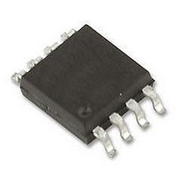
IC, VOLTAGE DETECTION, MSOP8
Manufacturer
Rohm Semiconductor
Series
-r
Type
Watchdog Circuitr
Specifications of BD87A41FVM-TR
Threshold Voltage
4.1V
No. Of Supervisors / Monitors
1
Supply Voltage Range
1V To 10V
Reset Type
Active-Low
Supply Current
5µA
Digital Ic Case Style
MSOP
No. Of Pins
8
Operating Temperature
RoHS Compliant
Number Of Voltages Monitored
1
Output
Open Drain or Open Collector
Reset
Active Low
Reset Timeout
Adjustable/Selectable
Voltage - Threshold
4.1V
Mounting Type
Surface Mount
Package / Case
8-VSSOP, 8-MSOP (0.110", 2.80mm Width)
Lead Free Status / Rohs Status
Lead free / RoHS Compliant
Available stocks
Company
Part Number
Manufacturer
Quantity
Price

Part Number:
BD87A41FVM-TR
Manufacturer:
ROHM/罗姆
Quantity:
20 000


© 2010 ROHM Co., Ltd. All rights reserved.
BD37A19FVM, BD37A41FVM, BD87A28FVM, BD87A29FVM,
BD87A34FVM, BD87A41FVM, BD99A41F
www.rohm.com
10) When VDD falls below the operating marginal voltage, output will be open. When output is being pulled up to input, output
11) Input pin
8) Ground Wiring Pattern
9) Applications or inspection processes with modes where the potentials of the VDD pin and other pins may be reversed from
When using both small signal and large current GND patterns, it is recommended to isolate the two ground patterns,
placing a single ground point at the ground potential of application so that the pattern wiring resistance and voltage
variations caused by large currents do not cause variations in the small signal ground voltage. Be careful not to change the
GND wiring pattern of any external components, either.
their normal states may cause damage to the IC’s internal circuitry or elements. Use an output pin capacitance of 1000 µF
or lower in case VDD is shorted with the GND pin while the external capacitor is charged. It is recommended to insert a
diode for preventing back current flow in series with VDD or bypass diodes between Vcc and each pin.
will be equivalent to VDD.
The CLK and INH pins comprise inverter gates and should not be left open. (These pins should be either pulled up or
down.) Input to the CLK pin is detected using a positive edge trigger and does not affect the CLK signal duty. Input the
trigger to the CLK pin within the TWH time.
Back current prevention diode
VDD
Fig.19
9/10
Pin
Bypass diode
Technical Note
2010.12 - Rev.A
Related parts for BD87A41FVM-TR
Image
Part Number
Description
Manufacturer
Datasheet
Request
R

Part Number:
Description:
Manufacturer:
Rohm Semiconductor
Datasheet:
Part Number:
Description:
Manufacturer:
Rohm Semiconductor
Datasheet:
Part Number:
Description:
Manufacturer:
Rohm Semiconductor
Datasheet:
Part Number:
Description:
Manufacturer:
Rohm Semiconductor
Datasheet:
Part Number:
Description:
Manufacturer:
Rohm Semiconductor
Datasheet:
Part Number:
Description:
Manufacturer:
Rohm Semiconductor
Datasheet:
Part Number:
Description:
Manufacturer:
Rohm Semiconductor
Datasheet:
Part Number:
Description:
Manufacturer:
Rohm Semiconductor
Datasheet:
Part Number:
Description:
Manufacturer:
Rohm Semiconductor
Datasheet:
Part Number:
Description:
Manufacturer:
Rohm Semiconductor
Datasheet:
Part Number:
Description:
Manufacturer:
Rohm Semiconductor
Datasheet:
Part Number:
Description:
Manufacturer:
Rohm Semiconductor
Datasheet:

Part Number:
Description:
DIODE SWITCH 80V 25MA SMD5 TR
Manufacturer:
Rohm Semiconductor
Datasheet: