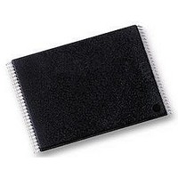
HY27UF082G2B-TPCB HYNIX SEMICONDUCTOR, HY27UF082G2B-TPCB Datasheet - Page 48

HY27UF082G2B-TPCB
Manufacturer Part Number
HY27UF082G2B-TPCB
Description
IC, MEMORY, FLASH NAND 2GB, TSOP48
Manufacturer
HYNIX SEMICONDUCTOR
Datasheet
1.HY27UF082G2B-TPCB.pdf
(54 pages)
Specifications of HY27UF082G2B-TPCB
Access Time
20ns
Supply Voltage Range
2.7V To 3.6V
Memory Case Style
TSOP
No. Of Pins
48
Operating Temperature Range
0°C To +70°C
Package / Case
TSOP
Base Number
27
Interface
Serial
Logic
RoHS Compliant
Memory Type
Flash - NAND
Memory Configuration
256M X 8
Rohs Compliant
Yes
Available stocks
Company
Part Number
Manufacturer
Quantity
Price
Company:
Part Number:
HY27UF082G2B-TPCB
Manufacturer:
PANASONIC
Quantity:
1 200
Company:
Part Number:
HY27UF082G2B-TPCB
Manufacturer:
HYNIX
Quantity:
2 526
Company:
Part Number:
HY27UF082G2B-TPCB
Manufacturer:
HY
Quantity:
744
Company:
Part Number:
HY27UF082G2B-TPCB
Manufacturer:
HYNIX
Quantity:
10 554
Part Number:
HY27UF082G2B-TPCB
Manufacturer:
HYNIX/海力士
Quantity:
20 000
Bad Block Replacement
Over the lifetime of the device additional Bad Blocks may develop. In this case the block has to be replaced by copying
the data to a valid block. These additional Bad Blocks can be identified as attempts to program or erase them will give
errors in the Status Register.
Unlike the case of odd page which carries a possibility of affecting previous page, the failure of a page program oper-
ation does not affect the data in other pages in the same block, the block can be replaced by re-programming the cur-
rent data and copying the rest of the replaced block to an available valid block.
Refer to Table 23 and Figure 32 for the recommended procedure to follow if an error occurs during an operation.
Rev 0.2 / Jan. 2008
NOTE :
1. An error occurs on n
2. Data in Block A is copied to same location in Block B which is valid block.
3. N
4. Bad block table should be updated to prevent from eraseing or programming Block A
th
data of block A which is in controller buffer memory is copied into n
Operation
Program
Erase
Read
th
page of the Block A during program or erase operation.
Figure 32: Bad Block Replacement
Table 23: Block Failure
Recommended Procedure
2Gbit (256Mx8bit) NAND Flash
ECC (with 1bit/528byte)
Block Replacement
Block Replacement
HY27UF(08/16)2G2B Series
th
page of Block B
48


