DS34LV87TM National Semiconductor, DS34LV87TM Datasheet

RS422/485 Line Driver IC

DS34LV87TM

Manufacturer Part Number
DS34LV87TM
Description
RS422/485 Line Driver IC
Manufacturer
National Semiconductor
Datasheet

Specifications of DS34LV87TM

Device Type
Line
No. Of Drivers
4
Driver Case Style
SOIC
No. Of Pins
16
Mounting Type
Surface Mount
Output Current Max
150mA
Peak Reflow Compatible (260 C)
No
Supply Voltage
5V
Interface Circuit Standard 1
EIA/TIA-422-B/RS-422
Number Of Receivers
Not Required
Number Of Transmitters
4
Number Of Transceivers
Not Required
Data Transmission Topology
Multidrop
Receiver Signal Type
Not Required
Transmitter Signal Type
Differential
Single Supply Voltage (typ)
3.3V
Single Supply Voltage (min)
3V
Single Supply Voltage (max)
3.6V
Dual Supply Voltage (typ)
Not RequiredV
Dual Supply Voltage (min)
Not RequiredV
Dual Supply Voltage (max)
Not RequiredV
Supply Current
0.1mA
Power Supply Requirement
Single
Operating Temp Range
-40C to 85C
Operating Temperature Classification
Industrial
Mounting
Surface Mount
Pin Count
16
Package Type
SOIC N
Lead Free Status / RoHS Status
Contains lead / RoHS non-compliant
Lead Free Status / RoHS Status
Contains lead / RoHS non-compliant

Available stocks

Company
Part Number
Manufacturer
Quantity
Price
Part Number:
DS34LV87TM
Manufacturer:
NS
Quantity:
850
Part Number:
DS34LV87TM
Manufacturer:
NS/国半
Quantity:
20 000
Part Number:
DS34LV87TM
Quantity:
144
Company:
Part Number:
DS34LV87TM
Quantity:
124
Part Number:
DS34LV87TMX/NOPB
Manufacturer:
TI/德州仪器
Quantity:
20 000
Part Number:
DS34LV87TMX/NOPB
0
© 2004 National Semiconductor Corporation
DS34LV87T
Enhanced CMOS Quad Differential Line Driver
General Description
The DS34LV87T is a high speed quad differential CMOS
driver that meets the requirements of both TIA/EIA-422-B
and ITU-T V.11. The CMOS DS34LV87T features low static
I
and power conscious applications. The TRI-STATE
EN, allows the device to be disabled when the device is not
in use to minimize power. The dual enable scheme allows for
flexibility in turning devices on or off.
Protection diodes protect all the driver inputs against elec-
trostatic discharge. The driver and enable inputs (DI and EN)
are compatible with LVTTL and LVCMOS devices. Differen-
tial outputs have the same V
version. The outputs have enhanced ESD Protection provid-
ing greater than 7 kV tolerance.
Connection Diagram
CC
TRI-STATE
of 100 µA max which makes it ideal for battery powered
®
is a registered trademark of National Semiconductor Corporation.
See NS Package Number M16A
Order Number DS34LV87TM
Dual-In-Line Package
Top View
OD
(≥2V) guarantee as the 5V
DS012645
01264501
®
enable,
Features
n Meets TIA/EIA-422-B (RS-422) and ITU-T V.11
n Interoperable with existing 5V RS-422 networks
n Guaranteed V
n Balanced output crossover for low EMI (typical within 40
n Low power design (330 µW
n ESD ≥ 7 kV on cable I/O pins (HBM)
n Industrial temperature range
n Guaranteed AC parameter:
n Pin compatible with DS26C31
n Available in SOIC packaging
Truth Table
L = Low logic state
X = Irrelevant
H = High logic state
Z = TRI-STATE
recommendation
mV of 50% voltage level)
— Maximum driver skew: 2 ns
— Maximum transition time: 10 ns
Enables
EN
H
H
L
OD
Input
DI
H
X
L
of 2V min over operating conditions
@
DO+
H
Z
L
3.3V static)
Outputs
November 2000
www.national.com
DO−
H
Z
L

Related parts for DS34LV87TM

DS34LV87TM Summary of contents

Page 1

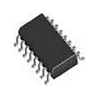
... OD version. The outputs have enhanced ESD Protection provid- ing greater than 7 kV tolerance. Connection Diagram Dual-In-Line Package Top View Order Number DS34LV87TM See NS Package Number M16A TRI-STATE ® registered trademark of National Semiconductor Corporation. © 2004 National Semiconductor Corporation Features n Meets TIA/EIA-422-B (RS-422) and ITU-T V ...

Page 2

... Absolute Maximum Ratings If Military/Aerospace specified devices are required, please contact the National Semiconductor Sales Office/ Distributors for availability and specifications. Supply Voltage ( Enable Input Voltage (EN) Driver Input Voltage ( Clamp Diode Current DC Output Current, per pin Driver Output Voltage (Power Off: DO+, DO−) ...

Page 3

Switching Characteristics Over Supply Voltage and Operating Temperature ranges, unless otherwise specified Symbol Parameter t Differential Propagation Delay PHLD High to Low t Differential Propagation Delay PLHD Low to High t Differential Skew SKD |t –t | PHLD PLHD t ...

Page 4

Parameter Measurement Information FIGURE 2. Differential Driver Propagation Delay and Transition Time Test Circuit FIGURE 3. Differential Driver Propagation Delay and Transition Time Waveforms Note 10: Generator waveform for all tests unless otherwise specified MHz, Duty Cycle ...

Page 5

Parameter Measurement Information FIGURE 5. Driver Single-Ended TRI-STATE Waveforms Typical Application Information General application guidelines and hints for differential driv- ers and receivers may be found in the following application notes: AN-214, AN-457, AN-805, AN-847, AN-903, AN-912, AN-916 ...

Page 6

Typical Application Information www.national.com (Continued) FIGURE 7. Typical Driver Output Waveforms 6 01264509 ...

Page 7

... National does not assume any responsibility for use of any circuitry described, no circuit patent licenses are implied and National reserves the right at any time without notice to change said circuitry and specifications. inches (millimeters) unless otherwise noted 16-Lead Molded Small Outline Package (M) Order Number DS34LV87TM NS Package Number M16A 2. A critical component is any component of a life ...

Related keywords