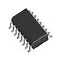
DS34LV87TM National Semiconductor, DS34LV87TM Datasheet - Page 3

DS34LV87TM
Manufacturer Part Number
DS34LV87TM
Description
RS422/485 Line Driver IC
Manufacturer
National Semiconductor
Datasheet
1.DS34LV87TM.pdf
(7 pages)
Specifications of DS34LV87TM
Device Type
Line
No. Of Drivers
4
Driver Case Style
SOIC
No. Of Pins
16
Mounting Type
Surface Mount
Output Current Max
150mA
Peak Reflow Compatible (260 C)
No
Supply Voltage
5V
Interface Circuit Standard 1
EIA/TIA-422-B/RS-422
Number Of Receivers
Not Required
Number Of Transmitters
4
Number Of Transceivers
Not Required
Data Transmission Topology
Multidrop
Receiver Signal Type
Not Required
Transmitter Signal Type
Differential
Single Supply Voltage (typ)
3.3V
Single Supply Voltage (min)
3V
Single Supply Voltage (max)
3.6V
Dual Supply Voltage (typ)
Not RequiredV
Dual Supply Voltage (min)
Not RequiredV
Dual Supply Voltage (max)
Not RequiredV
Supply Current
0.1mA
Power Supply Requirement
Single
Operating Temp Range
-40C to 85C
Operating Temperature Classification
Industrial
Mounting
Surface Mount
Pin Count
16
Package Type
SOIC N
Lead Free Status / RoHS Status
Contains lead / RoHS non-compliant
Lead Free Status / RoHS Status
Contains lead / RoHS non-compliant
Available stocks
Company
Part Number
Manufacturer
Quantity
Price
Company:
Part Number:
DS34LV87TM
Manufacturer:
NS
Quantity:
850
Part Number:
DS34LV87TM
Manufacturer:
NS/国半
Quantity:
20 000
Part Number:
DS34LV87TMX/NOPB
Manufacturer:
TI/德州仪器
Quantity:
20 000
t
t
t
t
t
t
t
t
t
t
t
f
Symbol
PHLD
PLHD
SKD
SK1
SK2
TLH
THL
PHZ
PLZ
PZH
PZL
MAX
Switching Characteristics
Over Supply Voltage and Operating Temperature ranges, unless otherwise specified
Note 1: “Absolute Maximum Ratings” are those values beyond which the safety of the device cannot be guaranteed. They are not meant to imply that the device
should be operated at these limits. The table of “Electrical Characteristics” specifies conditions of device operation.
Note 2: Current into device pins is defined as positive. Current out of device pins is defined as negative. All voltages are referenced to ground except differential
voltages V
Note 3: All typical values are given for V
Note 4: Only one output shorted at a time. The output (true or complement) is configured High.
Note 5: f = 1 MHz, t
Note 6: See TIA/EIA-422-B specifications for exact test conditions.
Note 7: This specification limit is for compliance with TIA/EIA-422-B and ITU-T V.11.
Note 8: Devices are at the same V
Note 9: All channels switching, output duty cycle criteria is 40%/60% measured at 50%. This parameter is guaranteed by design and characterization.
Parameter Measurement Information
OD1
Differential Propagation Delay
High to Low
Differential Propagation Delay
Low to High
Differential Skew
|t
Skew, Pin to Pin (same device)
Skew, Part to Part (Note 8)
Differential Transition Time
Low to High (20% to 80%)
Differential Transition Time
High to Low (80% to 20%)
Disable Time High to Z
Disable Time Low to Z
Enable Time Z to High
Enable Time Z to Low
Maximum Operating Frequency
(Note 9)
PHLD
, V
OD2
–t
r
, V
PLHD
and t
OD3
f
.
|
≤ 6 ns (10% to 90%).
CC
and within 5˚C within the operating temperature range.
Parameter
CC
= 3.3V and T
FIGURE 1. Differential Driver DC Test Circuit
(Notes 5, 6)
A
= +25˚C.
3
R
(Figures 2, 3)
(Figures 4, 5 )
L
= 100Ω, C
Conditions
L
= 50 pF
Min
6
6
01264502
10.5
Typ
0.5
1.0
3.0
4.2
4.7
11
12
22
22
32
9
Max
www.national.com
2.0
2.0
5.0
16
16
10
10
20
20
32
32
Units
MHz
ns
ns
ns
ns
ns
ns
ns
ns
ns
ns
ns


