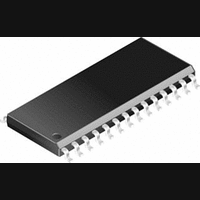
DS92LV1021TMSA National Semiconductor, DS92LV1021TMSA Datasheet

DS92LV1021TMSA
Specifications of DS92LV1021TMSA
Available stocks
Related parts for DS92LV1021TMSA
DS92LV1021TMSA Summary of contents
Page 1
... Block Diagrams TRI-STATE ® registered trademark of National Semiconductor Corporation. © 2002 National Semiconductor Corporation due to charged cable conditions. The DS92LV1021 output pins may be TRI-STATE state. The PLL can lock to frequencies between 16 MHz and 40 MHz ...
Page 2
Block Diagrams (Continued) Functional Description The DS92LV1021 and DS92LV1210 is a 10-bit Serializer / Deserializer chipset designed to transmit data over a heavily loaded differential backplanes at clock speeds from 16 to 40MHz. It may also be used to drive ...
Page 3
... SYNC2, PWRDN, TCLK_R/F). For the Deserializer, TRI-STATE is entered when the REN pin is driven low. This will TRI-STATE the receiver output pins (ROUT0–ROUT9), LOCK and RCLK. Order Numbers NSID Function DS92LV1021TMSA Serializer DS92LV1210TMSA Deserializer 3 Package MSA28 MSA28 ...
Page 4
... Absolute Maximum Ratings If Military/Aerospace specified devices are required, please contact the National Semiconductor Sales Office/ Distributors for availability and specifications. Supply Voltage ( CMOS/TTL Input Voltage −0. CMOS/TTL Output Voltage −0. Bus LVDS Receiver Input Voltage Bus LVDS Driver Output Voltage Bus LVDS Output Short ...
Page 5
Electrical Characteristics Over recommended operating supply and temperature ranges unless otherwise specified. Symbol Parameter I Input Current IN SERIALIZER SUPPLY CURRENT (apply to pins DVCC and AVCC) I Serializer Supply Current CCD Worst Case I Serializer Supply Current Powerdown PWRDN ...
Page 6
Deserializer Timing Requirements for REFCLK Over recommended operating supply and temperature ranges unless otherwise specified. Symbol Parameter t REFCLK Period RFCP t REFCLK Duty Cycle RFDC t / Ratio of REFCLK to RFCP t TCLK Periods TCP t REFCLK Transition ...
Page 7
AC Timing Diagrams and Test Circuits FIGURE 1. “Worst Case” Serializer ICC Test Pattern FIGURE 2. “Worst Case” Deserializer ICC Test Pattern FIGURE 3. Serializer Bus LVDS Output Load and Transition Times FIGURE 4. Deserializer CMOS/TTL Output Load and Transition ...
Page 8
AC Timing Diagrams and Test Circuits Timing shown for TCLK_R/F = LOW FIGURE 7. Serializer TRI-STATE Test Circuit and Timing www.national.com (Continued) FIGURE 5. Serializer Input Clock Transition Time FIGURE 6. Serializer Setup/Hold Times 8 10011007 10011008 10011009 ...
Page 9
AC Timing Diagrams and Test Circuits FIGURE 8. Serializer PLL Lock Time, SYNC Timing and PWRDN TRI-STATE Delays (Continued) FIGURE 9. Serializer Delay FIGURE 10. Deserializer Delay 9 10011010 10011011 10011012 www.national.com ...
Page 10
AC Timing Diagrams and Test Circuits Timing shown for RCLK_R/F = LOW Duty Cycle ( RDC FIGURE 12. Deserializer TRI-STATE Test Circuit and Timing www.national.com (Continued) FIGURE 11. Deserializer Setup and Hold Times 10 10011013 10011014 ...
Page 11
AC Timing Diagrams and Test Circuits FIGURE 13. Deserializer PLL Lock Times and PWRDN TRI-STATE Delays FIGURE 14. Deserializer PLL Lock Time from SyncPAT (Continued) 11 10011015 10011022 www.national.com ...
Page 12
AC Timing Diagrams and Test Circuits SW - Setup and Hold Time (Internal data sampling window Serializer Output Bit Position Jitter JIT t = Receiver Sampling Margin Time RSM + − (DO )–( Differential ...
Page 13
Application Information USING THE DS92LV1021 AND DS92LV1210 The Serializer and Deserializer chipset is an easy to use transmitter and receiver pair that sends 10 bits of parallel TTL data over a serial Bus LVDS link up to 400 Mbps. Serialization ...
Page 14
... Pin Diagrams www.national.com DS92LV1021TMSA - Serializer 10011018 DS92LV1210TMSA - Deserializer 10011019 14 ...
Page 15
Serializer Pin Description Pin Name I/O DIN I TCLK_R/F I DO+ O DO− O DEN I PWRDN I TCLK I SYNC I DVCC I DGND I AVCC I AGND I No. 3–12 Data Input. TTL levels inputs. Data on these ...
Page 16
Deserializer Pin Description Pin Name I/O ROUT O RCLK_R/F I RI+ I RI− I PWRDN I LOCK O RCLK O REN I DVCC I DGND I AVCC I AGND I REFCLK I www.national.com No. ± 15–19, 24–28 Data Output. 9 ...
Page 17
Truth Table DIN (0–9) TCLK_R/F TCLK SYSTEM CLK L DATA 1 K DATA 0 RI RI− RCLK_R SYNC PTRN SYNC X PTRN* DATA (0–9) DATA (0–9)* ...
Page 18
... Physical Dimensions Order Number DS92LV1021TMSA or DS92LV1210TMSA LIFE SUPPORT POLICY NATIONAL’S PRODUCTS ARE NOT AUTHORIZED FOR USE AS CRITICAL COMPONENTS IN LIFE SUPPORT DEVICES OR SYSTEMS WITHOUT THE EXPRESS WRITTEN APPROVAL OF THE PRESIDENT AND GENERAL COUNSEL OF NATIONAL SEMICONDUCTOR CORPORATION. As used herein: 1. Life support devices or systems are devices or ...


