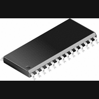
DS92LV1021TMSA National Semiconductor, DS92LV1021TMSA Datasheet - Page 5

DS92LV1021TMSA
Manufacturer Part Number
DS92LV1021TMSA
Description
Communication IC
Manufacturer
National Semiconductor
Datasheet
1.DS92LV1021TMSA.pdf
(18 pages)
Specifications of DS92LV1021TMSA
Peak Reflow Compatible (260 C)
No
Data Rate Max
400Mbps
Leaded Process Compatible
No
Mounting Type
Surface Mount
Package / Case
28-SSOP
Number Of Elements
1
Number Of Receivers
10
Number Of Drivers
1
Input Type
CMOS/TTL
Operating Supply Voltage (typ)
3.3V
Output Type
Serializer
Differential Output Voltage
270mV
Transmission Data Rate
400Mbps
Power Dissipation
1.27W
Operating Temp Range
-40C to 85C
Operating Temperature Classification
Industrial
Mounting
Surface Mount
Pin Count
28
Package Type
SSOP-EIAJ
Lead Free Status / RoHS Status
Contains lead / RoHS non-compliant
Lead Free Status / RoHS Status
Contains lead / RoHS non-compliant
Available stocks
Company
Part Number
Manufacturer
Quantity
Price
Company:
Part Number:
DS92LV1021TMSA
Manufacturer:
NS
Quantity:
274
Part Number:
DS92LV1021TMSA
Manufacturer:
NS/国半
Quantity:
20 000
Company:
Part Number:
DS92LV1021TMSA/NOPB
Manufacturer:
TI
Quantity:
16 000
Part Number:
DS92LV1021TMSAX
Manufacturer:
NS/国半
Quantity:
20 000
Company:
Part Number:
DS92LV1021TMSAX /NOPB
Manufacturer:
TI
Quantity:
16 000
I
SERIALIZER SUPPLY CURRENT (apply to pins DVCC and AVCC)
I
I
DESERIALIZER SUPPLY CURRENT (apply to pins DVCC and AVCC)
I
I
t
t
t
t
t
t
t
t
t
t
t
t
t
t
t
t
t
IN
CCD
CCXD
CCR
CCXR
TCP
TCIH
TCIL
CLKT
JIT
LLHT
LHLT
DIS
DIH
HZD
LZD
ZHD
ZLD
SPW
PLD
SD
BIT
Symbol
Symbol
Electrical Characteristics
Over recommended operating supply and temperature ranges unless otherwise specified.
Serializer Timing Requirements for TCLK
Over recommended operating supply and temperature ranges unless otherwise specified.
Serializer Switching Characteristics
Over recommended operating supply and temperature ranges unless otherwise specified.
Symbol
Transmit Clock Period
Transmit Clock High Time
Transmit Clock Low Time
TCLK Input Transition
Time
TCLK Input Jitter
Bus LVDS Low-to-High
Transition Time
Bus LVDS High-to-Low
Transition Time
DIN (0-9) Setup to TCLK
DIN (0-9) Hold from
TCLK
DO
TRI-STATE Delay
DO
TRI-STATE Delay
DO
HIGH Delay
DO
LOW Delay
SYNC Pulse Width
Serializer PLL Lock Time
Serializer Delay
Bus LVDS Bit Width
Input Current
Serializer Supply Current
Worst Case
Serializer Supply Current Powerdown PWRDN = 0.8V
Deserializer Supply Current
Worst Case
Deserializer Supply Current
Powerdown
±
±
±
±
HIGH to
LOW to
TRI-STATE to
TRI-STATE to
Parameter
Parameter
Parameter
R
Figure 3
C
Figure 6
R
C
Figure 7 (Note 4)
R
C
Figure 8
R
Figure 9 R
R
C
L
L
L
L
L
L
L
L
L
=10pF to GND
=10pF to GND
=10pF to GND
=10pF to GND
= 27Ω
= 27Ω,
= 27Ω,
= 27Ω
= 27Ω,
Conditions
Conditions
(Continued)
L
= 27Ω
V
V
RL = 27Ω
Figure 1
C
Figure 2
PWRDN = 0.8V, REN = 0.8V
IN
IN
L
= 15 pF
= +2.4V, V
= 0V, V
CC
5
CC
= 3.6V or 0V
1024*t
2048*t
Conditions
= 3.6V or 0V
0.4T
0.4T
t
Min
Min
1.0
6.5
TCP
25
TCP
TCP
f = 40 MHz
f = 16 MHz
f = 40 MHz
f = 16 MHz
t
TCP
t
CLK
0.5T
0.5T
0.25
Typ
Typ
0.2
4.5
3.5
2.9
2.5
2.7
T
3
0
+ 2.5
/ 12
Min
−10
−15
150
1029*t
2049*t
t
Typ
1.5
TCP
±
±
32
25
44
31
4
Max
62.5
0.6T
0.6T
Max
1
1
10
10
10
10
6
1
1
+ 5
TCP
TCP
Max
+10
+15
www.national.com
5.0
55
45
10
75
55
Units
Units
Units
ns
ns
ns
ns
ps
ns
ns
ns
ns
ns
ns
ns
ns
ns
ns
ns
ns
mA
mA
mA
mA
mA
mA
µA
µA


