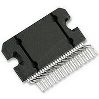
LM4781TA National Semiconductor, LM4781TA Datasheet - Page 8

LM4781TA
Manufacturer Part Number
LM4781TA
Description
Audio Power Amplifier IC
Manufacturer
National Semiconductor
Datasheet
1.LM4781TA.pdf
(25 pages)
Specifications of LM4781TA
Amplifier Case Style
TO-220
Peak Reflow Compatible (260 C)
No
Termination Type
Through Hole
Supply Voltage Max
56V
Leaded Process Compatible
No
Package / Case
27-TO-220
Operational Class
Class-AB
Audio Amplifier Output Configuration
3-Channel Stereo
Output Power (typ)
35x3@8OhmW
Audio Amplifier Function
Speaker
Input Offset Voltage
10@±28VmV
Input Bias Current
1uA
Total Harmonic Distortion
0.2@8Ohm@20W%
Single Supply Voltage (typ)
18V
Dual Supply Voltage (typ)
±12/±15/±18/±24/±28V
Power Supply Requirement
Single/Dual
Power Dissipation
125W
Unity Gain Bandwidth Product (typ)
8MHz
Rail/rail I/o Type
No
Power Supply Rejection Ratio
125dB
Single Supply Voltage (min)
20V
Single Supply Voltage (max)
70V
Dual Supply Voltage (min)
±10V
Dual Supply Voltage (max)
±35V
Operating Temp Range
-20C to 85C
Operating Temperature Classification
Commercial
Mounting
Through Hole
Pin Count
27 +Tab
Package Type
TO-220
Lead Free Status / RoHS Status
Contains lead / RoHS non-compliant
Lead Free Status / RoHS Status
Contains lead / RoHS non-compliant
Available stocks
Company
Part Number
Manufacturer
Quantity
Price
Company:
Part Number:
LM4781TA
Manufacturer:
IR
Quantity:
30 000
Part Number:
LM4781TA
Manufacturer:
NS/国半
Quantity:
20 000
Company:
Part Number:
LM4781TA/NOPB
Manufacturer:
National Semiconductor
Quantity:
135
www.national.com
10
12
13
14
15
16
17
18
19
20
21
22
23
24
11
External Components Description
(Figures 1-5)
1
2
3
4
5
6
7
8
9
Note 16: Optional components dependent upon specific design requirements.
Components
R
R
R
R
(Note 16)
C
(Note 16)
C
(Note 16)
C
(Note 16)
C
R
(Note 16)
R
(Note 16)
C
(Note 16)
R
(Note 16)
C
(Note 16)
L (Note 16)
R (Note 16)
R
C
R
(Note 16)
R
R
R
C
S
R
1
B
i
f
f2
f
C
i
S
V
IN
IN
SN
SN
A
A
INP
BI
E
M
M
OUT
Prevents current from entering the amplifier’s non-inverting input. This current may pass through to the load
during system power down, because of the amplifier’s low input impedance when the undervoltage circuitry
is off. This phenomenon occurs when the V
Inverting input resistance. Along with R
Feedback resistance. Along with R
Feedback resistance. Works with Cf and Rf creating a lowpass filter that lowers AC gain at high
frequencies. The -3dB point of the pole occurs when: (R
Non-Inverting configuration shown in Figure 5.
Compensation capacitor. Works with R
Compensation capacitor. Reduces the gain at higher frequencies to avoid quasi-saturation oscillations of the
output transistor. Also suppresses external electromagnetic switching noise created from fluorescent lamps.
Feedback capacitor which ensures unity gain at DC. Along with R
1/(2πR
Provides power supply filtering and bypassing. Refer to the Supply Bypassing application section for proper
placement and selection of bypass capacitors.
Acts as a volume control by setting the input voltage level.
Sets the amplifier’s input terminals DC bias point when C
create a highpass filter at f
the outputs when the inputs are floating. Recommended values are 10kΩ to 47kΩ. Refer to Figure 5.
Input capacitor. Prevents the input signal’s DC offsets from being passed onto the amplifier’s inputs.
Works with C
Works with R
pole is set at f
Provides high impedance at high frequencies so that R may decouple a highly capacitive load and reduce
the Q of the series resonant circuit. Also provides a low impedance at low frequencies to short out R and
pass audio signals to the load. Refer to Figure 5.
Provides DC voltage biasing for the transistor Q1 in single supply operation.
Provides bias filtering for single supply operation.
Limits the voltage difference between the amplifier’s inputs for single supply operation. Refer to the Clicks
and Pops application section for a more detailed explanation of the function of R
Provides input bias current for single supply operation. Refer to the Clicks and Pops application section for
a more detailed explanation of the function of R
Establishes a fixed DC current for the transistor Q1 in single supply operation. This resistor stabilizes the
half-supply point along with C
Mute resistance set up to allow 0.5mA to be drawn from each MUTE pin to turn the muting function off.
→ R
Current curves in the Typical Performance Characteristics section.
Mute capacitance set up to create a large time constant for turn-on and turn-off muting.
Mute switch. When open or switched to GND, the amplifier will be in mute mode.
Reduces current flow between outputs that are caused by Gain or DC offset differences between the
amplifiers.
M
i
is calculated using: R
C
i
).
SN
SN
C
= 1/(2πR
to stabilize the output stage by creating a pole that reduces high frequency instabilities.
to stabilize the output stage by creating a pole that reduces high frequency instabilities. The
SN
C
C
M
= 1/(2πR
SN
A
≤ (|V
.
). Refer to Figure 5.
i
, sets AC gain.
EE
| − 2.6V)/l where l ≥ 0.5mA. Refer to the Mute Attenuation vs Mute
IN
f
f
, sets AC gain.
C
and R
IN
Functional Description
8
). If the value of R
+
and V
f2
BI
to reduce AC gain at higher frequencies.
.
-
supply voltages are below 1.5V.
f
- R
IN
is present in the circuit. Also works with C
i
)/2 = R
IN
is too large, oscillations may be observed on
i
also creates a highpass filter at f
f
// [1/(2πf
c
C
f
) + R
INP
.
f2
] for the
c
=
IN
to


