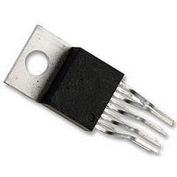
LM4950TS National Semiconductor, LM4950TS Datasheet

LM4950TS
Specifications of LM4950TS
Available stocks
Related parts for LM4950TS
LM4950TS Summary of contents
Page 1
... The LM4950 is a unity-gain stable and can be configured by external gain-setting resistors. Typical Application FIGURE 1. Typical Bridge-Tied-Load (BTL) Audio Amplifier Application Circuit Boomer ® registered trademark of National Semiconductor Corporation. © 2004 National Semiconductor Corporation Key Specifications j Quiscent Power Supply Current j P ...
Page 2
... Connection Diagrams www.national.com Plastic Package, TO-263 Top View U = Wafer Fab Code Z = Assembly Plant Code XY = Date Code TT = Die Traceability Order Number LM4950TS See NS Package Number TS9A Plastic Package, TO-220 Top View U = Wafer Fab Code Z = Assembly Plant Code XY = Date Code TT = Die Traceability Order Number LM4950TA ...
Page 3
... Absolute Maximum Ratings If Military/Aerospace specified devices are required, please contact the National Semiconductor Sales Office/ Distributors for availability and specifications. Supply Voltage (pin 6, referenced to GND, pins 4 and 5) Storage Temperature Input Voltage pins 3 and 7 pins and 9 Power Dissipation (Note 3) ESD Susceptibility (Note 4) ...
Page 4
Electrical Characteristics V Note 6: Typicals are measured at 25˚C and represent the parametric norm. Note 7: Limits are guaranteed to National’s AOQL (Average Outgoing Quality Level). Note 8: Datasheet min/max specification limits are guaranteed by design, test, or statistical ...
Page 5
Typical Performance Characteristics THD+N vs Frequency V = 12V 8Ω BTL operation, P OUT THD+N vs Frequency V = 12V 8Ω BTL operation, P OUT THD+N vs Frequency V = 12V, R ...
Page 6
Typical Performance Characteristics THD+N vs Frequency V = 12V 4Ω, SE operation both channels driven and loaded (average shown 1W, A OUT V THD+N vs Frequency V = 12V 8Ω, SE operation, ...
Page 7
Typical Performance Characteristics THD+N vs Output Power V = 12V 4Ω, SE operation both channels driven and loaded (average shown 1kHz IN THD+N vs Output Power V = 12V 16Ω, SE operation, ...
Page 8
Typical Performance Characteristics Output Power vs Power Supply Voltage R = 4Ω, SE operation, L both channels driven and loaded (average shown), at (from top to bottom at 12V): THD+N = 10%, THD Power Supply Rejection vs Frequency ...
Page 9
Typical Performance Characteristics Total Power Dissipation vs Load Dissipation V = 12V, BTL operation (from top to bottom at 3W 8Ω 16Ω Output Power vs Load Resistance V = 12V, BTL ...
Page 10
Typical Performance Characteristics THD+N vs Output Power V = 9.6V BTL operation THD+N vs Output Power V = 9.6V 8Ω, BTL operation BTLA = 20 1kHz V IN Total ...
Page 11
Typical Performance Characteristics Output Power vs Load Resistance V = 9.6V, BTL operation (from top to bottom at 15Ω): THD+N = 10%, THD Channel-to Channel Crosstalk vs Frequency V = 9.6V 4Ω, P ...
Page 12
Typical Performance Characteristics THD+N vs Output Power V = 15V operation both channels driven and loaded (average shown) Total Power Dissipation vs Load Dissipation per Channel V = 15V, SE operation ...
Page 13
Typical Performance Characteristics THD+N vs Output Power V = 16V 8Ω BTL operation 1kHz, BTLA IN Channel-to-Channel Crosstalk vs Frequency V = 16V 4Ω 1W, SE operation DD L OUT ...
Page 14
Typical Performance Characteristics Clipping Voltage vs Power Supply Voltage R = 8Ω, BTL operation (from top to bottom at 12V): positive signal swing, negative signal swing Clipping Voltage vs Power Supply Voltage R = 4Ω, SE operation, ...
Page 15
Application Information HIGH VOLTAGE BOOMER WITH INCREASED OUTPUT POWER Unlike previous 5V Boomer ® amplifiers, the LM4950 is de- signed to operate over a power supply voltages range of 9.6V to 16V. Operating on a 12V power supply, the LM4950 ...
Page 16
Application Information (2π Single Ended DMAX- The LM4950’s dissipation is twice the value given by Equa- tion (2) when driving two SE loads. For a 12V supply and two ...
Page 17
Application Information SELECTING EXTERNAL COMPONENTS Input Capacitor Value Selection Two quantities determine the value of the input coupling capacitor: the lowest audio frequency that requires amplifi- cation and desired output transient suppression. As shown in Figure 3, the input resistor ...
Page 18
Application Information FIGURE 4. Piezo-electric Transducer Capacitance ≤ 200nF AUDIO POWER AMPLIFIER DESIGN Audio Amplifier Design: Driving 4W into an 8Ω BTL The following are the desired operational parameters: Power Output Load Impedance Input Level Input Impedance Bandwidth 50Hz–20kHz The ...
Page 19
Application Information and 20kHz 100kHz L As mentioned in the SELECTING EXTERNAL COMPO- NENTS section, R and C create a highpass filter that INA INA sets the amplifier’s lower bandpass frequency limit. Find the ...
Page 20
Demonstration Board Layout www.national.com (Continued) FIGURE 6. Recommended TS SE PCB Layout: Top Layer FIGURE 7. Recommended TS SE PCB Layout: Bottom Layer 20 20047064 20047065 ...
Page 21
Demonstration Board Layout FIGURE 8. Recommended TS BTL PCB Layout: FIGURE 9. Recommended TS BTL PCB Layout: (Continued) 20047066 Top Silkscreen 20047067 Top Layer 21 www.national.com ...
Page 22
Demonstration Board Layout www.national.com (Continued) FIGURE 10. Recommended TS BTL PCB Layout: Bottom Layer 22 20047068 ...
Page 23
... Physical Dimensions inches (millimeters) unless otherwise noted Order Number LM4950TS NS Package Number TS9A 23 www.national.com ...
Page 24
Physical Dimensions www.national.com inches (millimeters) unless otherwise noted (Continued) For Staggered Lead Non-Isolated Package Order Number LM4950TA NS Package Number TA09A 24 ...
Page 25
... BANNED SUBSTANCE COMPLIANCE National Semiconductor certifies that the products and packing materials meet the provisions of the Customer Products Stewardship Specification (CSP-9-111C2) and the Banned Substances and Materials of Interest Specification (CSP-9-111S2) and contain no ‘‘Banned Substances’’ as defined in CSP-9-111S2. ...


