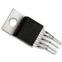
LM4950TS National Semiconductor, LM4950TS Datasheet - Page 18

LM4950TS
Manufacturer Part Number
LM4950TS
Description
Audio Power Amplifier IC
Manufacturer
National Semiconductor
Datasheet
1.LM4950TS.pdf
(25 pages)
Specifications of LM4950TS
Amplifier Case Style
TO-220
No. Of Pins
9
Peak Reflow Compatible (260 C)
No
Termination Type
Through Hole
Leaded Process Compatible
No
Package / Case
9-TO-220
Operational Class
Class-AB
Audio Amplifier Function
Speaker
Input Offset Voltage
30@12VmV
Total Harmonic Distortion
0.05@4Ohm@2.5W%
Single Supply Voltage (typ)
12/15V
Dual Supply Voltage (typ)
Not RequiredV
Power Supply Requirement
Single
Rail/rail I/o Type
No
Power Supply Rejection Ratio
70dB
Single Supply Voltage (min)
9.6V
Single Supply Voltage (max)
16V
Dual Supply Voltage (min)
Not RequiredV
Dual Supply Voltage (max)
Not RequiredV
Operating Temp Range
-40C to 85C
Operating Temperature Classification
Industrial
Mounting
Surface Mount
Pin Count
9 +Tab
Package Type
TO-263
Lead Free Status / RoHS Status
Contains lead / RoHS non-compliant
Lead Free Status / RoHS Status
Contains lead / RoHS non-compliant
Available stocks
Company
Part Number
Manufacturer
Quantity
Price
Part Number:
LM4950TS
Manufacturer:
NS/国半
Quantity:
20 000
Company:
Part Number:
LM4950TSX
Manufacturer:
INTEL
Quantity:
182
Part Number:
LM4950TSX
Manufacturer:
NS/国半
Quantity:
20 000
www.national.com
Application Information
AUDIO POWER AMPLIFIER DESIGN
Audio Amplifier Design: Driving 4W into an 8Ω BTL
The design begins by specifying the minimum supply voltage
necessary to obtain the specified output power. One way to
find the minimum supply voltage is to use the Output Power
vs Power Supply Voltage curve in the Typical Performance
Characteristics section. Another way, using Equation (8), is
to calculate the peak output voltage necessary to achieve
the desired output power for a given load impedance. To
account for the amplifier’s dropout voltage, two additional
voltages, based on the Clipping Dropout Voltage vs Power
Supply Voltage in the Typical Performance Characteris-
tics curves, must be added to the result obtained by Equa-
tion (8). The result is Equation (9).
The Output Power vs. Power Supply Voltage graph for an 8Ω
load indicates a minimum supply voltage of 10.2V. The com-
monly used 12V supply voltage easily meets this. The addi-
tional voltage creates the benefit of headroom, allowing the
LM4950 to produce peak output power in excess of 4W
without clipping or other audible distortion. The choice of
The following are the desired operational parameters:
Power Output
Load Impedance
Input Level
Input Impedance
Bandwidth
V
DD
= V
OUTPEAK
+ V
ODTOP
FIGURE 4. Piezo-electric Transducer Capacitance ≤ 200nF
50Hz–20kHz
+ V
(Continued)
ODBOT
0.3V
RMS
±
4W
0.25dB
(max)
20kΩ
RMS
8Ω
(8)
(9)
18
supply voltage must also not create a situation that violates
of maximum power dissipation as explained above in the
Power Dissipation section. After satisfying the LM4950’s
power dissipation requirements, the minimum differential
gain needed to achieve 4W dissipation in an 8Ω BTL load is
found using Equation (10).
Thus, a minimum gain of 18.9 allows the LM4950’s to reach
full output swing and maintain low noise and THD+N perfor-
mance. For this example, let A
overall BTL gain is set using the input (RIN
(R) resistors of the first amplifier in the series BTL configu-
ration. Additionaly, A
amplifier’s R
at 20kΩ, the feedback resistor is found using Equation (11).
The value of R
The nominal output power is 4W.
The last step in this design example is setting the amplifier’s
-3dB frequency bandwidth. To achieve the desired
pass band magnitude variation limit, the low frequency re-
sponse must extend to at least one-fifth the lower bandwidth
limit and the high frequency response must extend to at least
five times the upper bandwidth limit. The gain variation for
both response limits is 0.17dB, well within the
desired limit. The results are an
IN
f
and R
is 190kΩ (choose 191kΩ, the closest value).
f
R
L
V-BTL
f
. With the desired input impedance set
f
= 50Hz / 5 = 10Hz
/ R
IN
is twice the gain set by the first
= A
20047079
V-BTL
V-BTL
/ 2
= 19. The amplifier’s
A
) and feedback
±
±
0.25dB-
0.25dB
(10)
(12)
(11)


