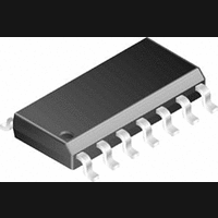
LMC6484IM National Semiconductor, LMC6484IM Datasheet - Page 5

LMC6484IM
Manufacturer Part Number
LMC6484IM
Description
Operational Amplifier (Op-Amp) IC
Manufacturer
National Semiconductor
Specifications of LMC6484IM
No. Of Amplifiers
4
Slew Rate
1.3V/µs
No. Of Pins
14
Amplifier Type
Operational
Mounting Type
Surface Mount
Peak Reflow Compatible (260 C)
No
Leaded Process Compatible
No
Number Of Channels
4
Voltage Gain Db
116.47 dB
Common Mode Rejection Ratio (min)
65 dB
Input Offset Voltage
3 mV at 5 V
Operating Supply Voltage
5 V, 9 V, 12 V, 15 V
Supply Current
2.8 mA at 5 V
Maximum Operating Temperature
+ 85 C
Package / Case
SOIC-14 Narrow
Minimum Operating Temperature
- 40 C
Lead Free Status / RoHS Status
Contains lead / RoHS non-compliant
Available stocks
Company
Part Number
Manufacturer
Quantity
Price
Company:
Part Number:
LMC6484IM
Manufacturer:
NS
Quantity:
16 600
Part Number:
LMC6484IM
Manufacturer:
NS/国半
Quantity:
20 000
Part Number:
LMC6484IMX
Manufacturer:
NS/国半
Quantity:
20 000
Company:
Part Number:
LMC6484IMX/NOPB
Manufacturer:
NS
Quantity:
1 000
Part Number:
LMC6484IMX/NOPB
Manufacturer:
TI/德州仪器
Quantity:
20 000
AC Electrical Characteristics
Note 3: Applies to both single supply and split-supply operation. Continuous short circuit operation at elevated ambient temperature can result in exceeding the maxi-
mum allowed junction temperature of 150˚C. Output currents in excess of
Note 4: The maximum power dissipation is a function of T
− T
Note 5: Typical Values represent the most likely parametric norm.
Note 6: All limits are guaranteed by testing or statistical analysis.
Note 7: V
Note 8: Do not short circuit output to V
Note 9: V
Note 10: Input referred, V
Note 11: Connected as Voltage Follower with 2V step input. Number specified is the slower of either the positive or negative slew rates.
Note 12: Limiting input pin current is only necessary for input voltages that exceed absolute maximum input voltage ratings.
Note 13: Guaranteed limits are dictated by tester limitations and not device performance. Actual performance is reflected in the typical value.
Note 14: For guaranteed Military Temperature Range parameters see RETSMC6484X.
Typical Performance Characteristics
specified
Supply Current vs
Supply Voltage
Sourcing Current vs
Output Voltage
A
)/
JA
. All numbers apply for packages soldered directly into a PC board.
+
+
= 15V, V
= 15V. Connected as Voltage Follower with 10V step input. Number specified is the slower of either the positive or negative slew rates.
CM
= 7.5V and R
+
= 15V and R
DS011714-39
DS011714-42
L
+
connected to 7.5V. For Sourcing tests, 7.5V
, when V
L
= 100 k
+
is greater than 13V or reliability will be adversely affected.
connected to 7.5V. Each amp excited in turn with 1 kHz to produce V
Input Current vs
Temperature
Sourcing Current vs
Output Voltage
J(max)
,
(Continued)
JA
, and T
A
±
. The maximum allowable power dissipation at any ambient temperature is P
30 mA over long term may adversely affect reliability.
V
S
5
= +15V, Single Supply, T
V
O
11.5V. For Sinking tests, 3.5V
DS011714-43
DS011714-40
Sourcing Current vs
Output Voltage
Sinking Current vs
Output Voltage
A
= 25˚C unless otherwise
O
V
= 12 V
O
7.5V.
PP
.
www.national.com
DS011714-41
DS011714-44
D
= (T
J(max)


