MCP1630RD-DDBK1 Microchip Technology, MCP1630RD-DDBK1 Datasheet - Page 12
MCP1630RD-DDBK1
Manufacturer Part Number
MCP1630RD-DDBK1
Description
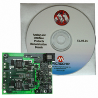
MCP1630 Dual Synchronous Buck Regulator Demo Board DEVTOOL - Analog
Manufacturer
Microchip Technology
Type
DC/DC Switching Converters, Regulators & Controllersr
Specifications of MCP1630RD-DDBK1
Main Purpose
DC/DC, Step Down
Outputs And Type
2, Non-Isolated
Voltage - Output
1.22 ~ 2.3V, 2.42 ~ 3.39V
Current - Output
20A, 20A
Voltage - Input
9 ~ 13.5V
Regulator Topology
Buck
Frequency - Switching
500kHz
Board Type
Fully Populated
Utilized Ic / Part
MCP1630
Input Voltage
12 V
Interface Type
Ethernet
Product
Power Management Modules
Lead Free Status / RoHS Status
Lead free / RoHS Compliant
Power - Output
-
Lead Free Status / Rohs Status
Lead free / RoHS Compliant
For Use With/related Products
MCP1630
Lead Free Status / RoHS Status
Lead free / RoHS Compliant, Contains lead / RoHS non-compliant


MCP1630 Dual Buck Reference Design
DS51531B-page 8
2.3.1
Powering the MCP1630 Dual Buck Reference Design.
1. Apply the input voltage to the connector (J3) provided. Connect the positive side
2. An on/off push-button switch (SW3) is used to turn the converter outputs on and
3. In the event of a fault, (input voltage out-of-range, output voltage out-of-range or
Applying the load to the MCP1630 Dual Buck Reference Design.
1. To apply a load to V
2. To apply a load to V
3. Outputs V
2.3.2
1. The MCP1630 Dual Buck Reference Design has two status LED’s. One LED
2. The second LED (D1) is used for fault and power good indication. During normal
Note:
of the input source (+) to the test point (J3-1). Connect the negative (or return
side (-)) of the input source to the GND terminal (J3-2). J3 is the center two
position terminal block located on the left side of the board. A 14-gauge wire size
is recommended for evaluating the board at 20A per output. The power supply
input voltage must be in the specified operating range for the board to operate.
An undervoltage lockout circuit prevents the converter from running when the
input voltage is too low.
off. During normal power-up, the outputs are turned on by pressing SW3 once.
To turn the outputs off, press SW3 again.
power train overtemperature), both V
by the D1 power good LED flashing. To restart, the input voltage must be brought
to 0V and raised back to the specified input voltage range of the converter prior
to pressing the on/off button. A solid D1 power good LED indicates that the
regulator outputs are operating properly at their programmed values.
the positive side of the V
(J2-2). The negative side of the V
GND (J2-1).
the positive side of the V
(J4-2). The negative side of the V
GND (J4-1).
Both outputs have independent over current protection, overtemperature and
short-circuit protection.
(D3) is used to determine if input voltage is present.
operation, if both regulator outputs are within regulation, D1 is illuminated to
provide indication that power is good. If either output is out of regulation, D1 will
blink, providing indication that one or both of the outputs are not in regulation.
Power Input and Output Connections
Power Present and Power Good Indication
The maximum rated load is 20A per output. When loading the board over
10A, airflow is necessary to prevent the overtemperature protection
circuitry from automatically turing off the power train that has the
overtemperature condition.
O1
and V
O2
OUT1
OUT2
are independent of each other and are loaded separately.
O1
O2
of the MCP1630 Dual Buck Reference Design,
of the MCP1630 Dual Buck Reference Design,
load (+) should be connected to the terminal +V
load (+) should be connected to the terminal +V
O1
O2
load should be connected to the terminal
load should be connected to the terminal
OUT1
and V
OUT2
will shut down, indicated
© 2008 Microchip Technology Inc.
O1
O2
Related parts for MCP1630RD-DDBK1
Image
Part Number
Description
Manufacturer
Datasheet
Request
R

Part Number:
Description:
REF DESIGN MCP1630 NIMH BATT CHG
Manufacturer:
Microchip Technology
Datasheet:

Part Number:
Description:
BOARD DEMO FOR MCP1630 LI-ION
Manufacturer:
Microchip Technology
Datasheet:

Part Number:
Description:
REF DESIGN MCP1630V BI-DIR 4CELL
Manufacturer:
Microchip Technology
Datasheet:

Part Number:
Description:
REFERENCE DESIGN FOR MCP1630
Manufacturer:
Microchip Technology
Datasheet:
Part Number:
Description:
Power Management IC Development Tools MCP1630 Sepic Automotive LED Drvr
Manufacturer:
Microchip Technology
Datasheet:

Part Number:
Description:
Manufacturer:
Microchip Technology Inc.
Datasheet:
Part Number:
Description:
Manufacturer:
Microchip Technology Inc.
Datasheet:
Part Number:
Description:
Manufacturer:
Microchip Technology Inc.
Datasheet:
Part Number:
Description:
Manufacturer:
Microchip Technology Inc.
Datasheet:
Part Number:
Description:
Manufacturer:
Microchip Technology Inc.
Datasheet:
Part Number:
Description:
Manufacturer:
Microchip Technology Inc.
Datasheet: