PIC16HV785-E/ML Microchip Technology, PIC16HV785-E/ML Datasheet - Page 24
PIC16HV785-E/ML
Manufacturer Part Number
PIC16HV785-E/ML
Description
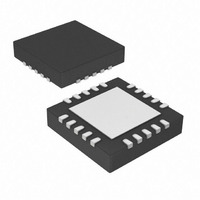
3.5KB Flash, 128 RAM, 18 I/O 20 QFN 4x4mm TUBE
Manufacturer
Microchip Technology
Series
PIC® 16Fr
Datasheets
1.PIC16F616T-ISL.pdf
(8 pages)
2.PIC16F785-ISS.pdf
(206 pages)
3.PIC16F785-ISS.pdf
(10 pages)
4.PIC16F785-ISS.pdf
(28 pages)
Specifications of PIC16HV785-E/ML
Core Processor
PIC
Core Size
8-Bit
Speed
20MHz
Peripherals
Brown-out Detect/Reset, POR, PWM, WDT
Number Of I /o
17
Program Memory Size
3.5KB (2K x 14)
Program Memory Type
FLASH
Eeprom Size
256 x 8
Ram Size
128 x 8
Voltage - Supply (vcc/vdd)
2 V ~ 5.5 V
Data Converters
A/D 14x10b
Oscillator Type
Internal
Operating Temperature
-40°C ~ 125°C
Package / Case
20-VQFN Exposed Pad, 20-HVQFN, 20-SQFN, 20-DHVQFN
Processor Series
PIC16H
Core
PIC
Data Bus Width
8 bit
Data Ram Size
128 B
Interface Type
RS- 232, USB
Maximum Clock Frequency
32 MHz
Number Of Programmable I/os
18
Number Of Timers
3
Maximum Operating Temperature
+ 125 C
Mounting Style
SMD/SMT
3rd Party Development Tools
52715-96, 52716-328, 52717-734
Development Tools By Supplier
PG164130, DV164035, DV244005, DV164005, PG164120, ICE2000, DV164120, DM163029
Minimum Operating Temperature
- 40 C
On-chip Adc
10 bit, 14 Channel
Lead Free Status / RoHS Status
Lead free / RoHS Compliant
For Use With
AC164324 - MODULE SKT FOR MPLAB 8DFN/16QFN
Connectivity
-
Lead Free Status / Rohs Status
Details
Available stocks
Company
Part Number
Manufacturer
Quantity
Price
Company:

Part Number:
PIC16HV785-E/ML
Manufacturer:
LEGERITY
Quantity:
100


PIC16F785/HV785
5.0
For the PIC16F785/HV785, once the CP bit is
programmed to ‘0’, all program memory locations read
all ‘0’s. The user ID locations and the Configuration
Word read out in an unprotected fashion. Further
programming is disabled for the entire program
memory.
Data memory is protected with its own code-protect bit
(CPD). When enabled, the data memory can still be
programmed and read using the EECON1 register.
The user ID locations and the Configuration Word can
be programmed regardless of the state of the CP and
CPD bits.
5.1
It is recommended to use the procedure in Figure 3-20
to disable code protection of the device. This sequence
will erase the program memory, data memory, Configu-
ration Word (0x2007) and user ID locations (0x2000-
0x2003). The Calibration Words (0x2008-0x2009) will
not be erased.
5.2
To allow portability of code, the programmer is required
to read the Configuration Word and user ID locations
from the hex file when loading the hex file. If Configura-
tion Word information was not present in the hex file, a
simple warning message may be issued. Similarly,
while saving a hex file, Configuration Word and user ID
information must be included. An option to not include
this information may be provided.
Specifically for the PIC16F785/HV785, the data
memory should also be embedded in the hex file (see
Section 5.3.2 “Embedding Data Memory Contents
in Hex File”).
Microchip Technology Incorporated feels strongly that
this feature is important for the benefit of the end
customer.
DS41237D-page 24
Note:
CODE PROTECTION
Disabling Code Protection
Embedding Configuration Word
and User ID Information in the Hex
File
To ensure system security, if CPD bit = 0,
Bulk Erase Program Memory command
will also erase data memory.
5.3
5.3.1
Checksum is calculated by reading the contents of the
PIC16F785/HV785 memory locations and adding up
the opcodes up to the maximum user addressable
location (e.g., 0x7FF for the PIC16F785/HV785). Any
Carry bits exceeding 16 bits are neglected. Finally, the
Configuration Word (appropriately masked) is added to
the checksum. Checksum computation for the
PIC16F785/HV785 devices is shown in Table 5-1.
The checksum is calculated by summing the following:
• The contents of all program memory locations
• The Configuration Word, appropriately masked
• Masked user ID locations (when applicable)
The 16 LSbs of this sum is the checksum.
The following table describes how to calculate the
checksum for each device. Note that the checksum
calculation differs depending on the code-protect
setting. Since the program memory locations read out
‘0’s when code-protected, the table describes how to
manipulate the actual program memory values to
simulate values that would be read from a protected
device. When calculating a checksum by reading a
device, the entire program memory can simply be read
and summed. The Configuration Word and user ID
locations can always be read regardless of code-protect
setting.
Note:
Checksum Computation
CHECKSUM
Some older devices have an additional
value added in the checksum. This is to
maintain compatibility with older device
programmer checksums.
2009 Microchip Technology Inc.
Related parts for PIC16HV785-E/ML
Image
Part Number
Description
Manufacturer
Datasheet
Request
R

Part Number:
Description:
Manufacturer:
Microchip Technology Inc.
Datasheet:
Part Number:
Description:
Manufacturer:
Microchip Technology Inc.
Datasheet:
Part Number:
Description:
Manufacturer:
Microchip Technology Inc.
Datasheet:
Part Number:
Description:
Manufacturer:
Microchip Technology Inc.
Datasheet:
Part Number:
Description:
Manufacturer:
Microchip Technology Inc.
Datasheet:
Part Number:
Description:
Manufacturer:
Microchip Technology Inc.
Datasheet:
Part Number:
Description:
Manufacturer:
Microchip Technology Inc.
Datasheet:
Part Number:
Description:
Manufacturer:
Microchip Technology Inc.
Datasheet: