A1210LUA-T Allegro Microsystems Inc, A1210LUA-T Datasheet

IC LATCH HALL EFFECT 3-SIP

A1210LUA-T

Manufacturer Part Number
A1210LUA-T
Description
IC LATCH HALL EFFECT 3-SIP
Manufacturer
Allegro Microsystems Inc
Type
Bipolar Latchr
Datasheet

Specifications of A1210LUA-T

Sensing Range
150G Trip, -150G Release
Voltage - Supply
3.8 V ~ 24 V
Current - Supply
7.5mA
Current - Output (max)
25mA
Output Type
Digital, Open Drain
Operating Temperature
-40°C ~ 150°C
Package / Case
3-SIP
Operate Point Typ
150G
Termination Type
SIP
No. Of Pins
3
Hall Effect Type
Latching
Supply Voltage Min
3.8V
Operating Temperature Max
150°C
Peak Reflow Compatible (260 C)
Yes
Supply Voltage
24V
Output Current
25mA
Sensor Case Style
SIP
Supply Voltage Range
3.8V To 24V
Operating Temperature Range
-40°C To +150°C
Svhc
No SVHC (15-Dec-2010)
Rohs Compliant
Yes
Magnetic Type
Latch
Operating Supply Voltage (min)
3.8V
Operating Supply Voltage (typ)
5/9/12/15/18V
Operating Supply Voltage (max)
24V
Mag Sensor Operate Point (g)
150Gs
Mag Sensor Release Point (g)
-150Gs
Mag Sensor Hysteresis(g)
155Gs
Package Type
Ultra Mini SIP
Pin Count
3
Mounting
Through Hole
Operating Temp Range
-40C to 150C
Operating Temperature Classification
Automotive
Filter Terminals
SIP
Leaded Process Compatible
Yes
Operating Temperature Min
-40°C
Lead Free Status / RoHS Status
Lead free / RoHS Compliant
Features
-
Lead Free Status / Rohs Status
Compliant
Other names
620-1014

Available stocks

Company
Part Number
Manufacturer
Quantity
Price
Part Number:
A1210LUA-T
Manufacturer:
ALLEGRO/雅丽高
Quantity:
20 000
Features and Benefits
▪ Continuous-time operation
▪ Stable operation over full operating temperature range
▪ Reverse battery protection
▪ Solid-state reliability
▪ Factory-programmed at end-of-line for optimum
▪ Robust EMC performance
▪ High ESD rating
▪ Regulator stability without a bypass capacitor
Packages: 3 pin SOT23W (suffix LH), and
3 pin SIP (suffix UA)
A1210-DS, Rev. 9
Not to scale
▫ Fast power-on time
▫ Low noise
performance
1
2
3
VCC
1
2
3
Functional Block Diagram
Regulator
Gain
Continuous-Time Latch Family
Amp
To all subcircuits
A1210, A1211, A1212, A1213, and A1214
Control
Trim
Description
The Allegro
generation replacements for the popular Allegro 317x and
318x lines of latching switches. The A121x family, pro-
duced with BiCMOS technology, consists of devices that
feature fast power-on time and low-noise operation. Device
programming is performed after packaging, to ensure
increased switchpoint accuracy by eliminating offsets that
can be induced by package stress. Unique Hall element
geometries and low-offset amplifiers help to minimize noise
and to reduce the residual offset voltage normally caused by
device overmolding, temperature excursions, and thermal
stress.
The A1210-A1214 Hall-effect latches include the following
on a single silicon chip: voltage regulator, Hall-voltage gen-
erator, small-signal amplifier, Schmitt trigger, and NMOS
output transistor. The integrated voltage regulator permits
operation from 3.8 to 24 V. The extensive on-board protec-
tion circuitry makes possible a ±30 V absolute maximum
voltage rating for superior protection in automotive and
industrial motor commutation applications, without adding
external components. All devices in the family are identical
except for magnetic switchpoint levels.
The small geometries of the BiCMOS process allow these
devices to be provided in ultrasmall packages. The package
styles available provide magnetically optimized solutions
for most applications. Package LH is an SOT23W, a min-
iature low-profile surface-mount package, while package
UA is a three-lead ultramini SIP for through-hole mounting.
Each package is lead (Pb) free, with 100% matte tin plated
leadframes.
Offset
®
A1210-A1214 Hall-effect latches are next
GND
VOUT

Related parts for A1210LUA-T

A1210LUA-T Summary of contents

Page 1

Features and Benefits ▪ Continuous-time operation ▫ Fast power-on time ▫ Low noise ▪ Stable operation over full operating temperature range ▪ Reverse battery protection ▪ Solid-state reliability ▪ Factory-programmed at end-of-line for optimum performance ▪ Robust EMC performance ▪ ...

Page 2

... A1212, A1213, A1214 and Selection Guide Part Number Packing* A1210ELHLT-T 7-in. reel, 3000 pieces/reel A1210LLHLT-T 7-in. reel, 3000 pieces/reel A1210LUA-T Bulk, 500 pieces/bag A1211LUA-T Bulk, 500 pieces/bag A1212LLHLT-T 7-in. reel, 3000 pieces/reel A1212LUA-T Bulk, 500 pieces/bag A1213LLHLT-T 7-in. reel, 3000 pieces/reel ...

Page 3

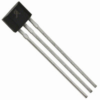
A1210, A1211, A1212, A1213, A1214 and Package LH, 3-pin Surface Mount 3 1 Terminal List Name VCC Connects power supply to chip VOUT Output from circuit GND Ground Continuous-Time Latch Family Pin-out Diagrams 2 Description Package UA, 3-pin SIP 2 ...

Page 4

A1210, A1211, A1212, A1213, A1214 and OPERATING CHARACTERISTICS over full operating voltage and ambient temperature ranges, unless otherwise noted Characteristic Symbol Electrical Characteristics 1 Supply Voltage V Output Leakage Current I OUTOFF Output On Voltage V OUT(SAT) Power-On Time 2 ...

Page 5

A1210, A1211, A1212, A1213, A1214 and THERMAL CHARACTERISTICS may require derating at maximum conditions, see application information Characteristic Package Thermal Resistance Continuous-Time Latch Family Symbol Package LH, on single layer, single-sided PCB with copper limited to solder pads Package LH, ...

Page 6

A1210, A1211, A1212, A1213, A1214 and Supply Current (On) versus Ambient Temperature (A1210/11/12/13/14) 8.0 7.0 6.0 5.0 4.0 3.0 2.0 1.0 0 – (°C) A Supply Current (Off) versus Ambient Temperature (A1210/11/12/13/14) 8.0 7.0 6.0 5.0 4.0 ...

Page 7

A1210, A1211, A1212, A1213, A1214 and Operate Point versus Ambient Temperature (A1210) 150 125 100 – (°C) A Release Point versus Ambient Temperature (A1210) -25 -50 -75 -100 -125 -150 – ...

Page 8

A1210, A1211, A1212, A1213, A1214 and Operate Point versus Ambient Temperature (A1211) 165 140 115 – (°C) A Release Point versus Ambient Temperature (A1211) -30 -55 -80 -105 -130 -155 -180 –50 0 ...

Page 9

A1210, A1211, A1212, A1213, A1214 and OPERATION The output of these devices switches low (turns on) when a magnetic field perpendicular to the Hall element exceeds the operate point threshold After turn-on, the output is capable OP of ...

Page 10

A1210, A1211, A1212, A1213, A1214 and ADDITIONAL APPLICATIONS INFORMATION Extensive applications information for Hall-effect devices is available in: • Hall-Effect IC Applications Guide, Application Note 27701 • Hall-Effect Devices: Gluing, Potting, Encapsulating, Lead Welding and Lead Forming, Application Note 27703.1 ...

Page 11

A1210, A1211, A1212, A1213, A1214 and Power Derating The device must be operated below the maximum junction temperature of the device Under certain combinations of J(max) peak conditions, reliable operation may require derating sup- plied power or improving ...

Page 12

A1210, A1211, A1212, A1213, A1214 and +0.12 2.98 –0.08 3 +0.10 2.90 –0. 10° REF 0.95 BSC For Reference Only; not for tooling use (reference dwg. 802840) Dimensions in millimeters Dimensions exclusive of mold flash, gate burrs, and ...

Page 13

A1210, A1211, A1212, A1213, A1214 and 4.09 45° +0.08 3.02 –0.05 2.16 MAX 0.51 REF 1 2 15.75 ±0.51 +0.05 0.43 –0.07 Copyright ©2005-2010, Allegro MicroSystems, Inc. Allegro MicroSystems, Inc. reserves the right to make, from time to time, such ...

Related keywords