TLV4946K Infineon Technologies, TLV4946K Datasheet
TLV4946K
Specifications of TLV4946K


Related parts for TLV4946K

TLV4946K Summary of contents
Page 1
TLV4946- ...
Page 2
... Infineon Technologies Office. Infineon Technologies components may be used in life-support devices or systems only with the express written approval of Infineon Technologies failure of such components can reasonably be expected to cause the failure of that life-support device or system or to affect the safety or effectiveness of that device or system. Life support devices or systems are intended to be implanted in the human body or to support and/or maintain and sustain and/or protect human life ...
Page 3
... Previous Revisions: none Page Subjects (major changes since last revision) all TLV4946K and TLV4946-2K removed We Listen to Your Comments Any information within this document that you feel is wrong, unclear or missing at all? Your feedback will help us to continuously improve the quality of this document. ...
Page 4
... Operating Modes and States . . . . . . . . . . . . . . . . . . . . . . . . . . . . . . . . . . . . . . . . . . . . . . . . . . . . . . . 10 2.6 Functional Block Description . . . . . . . . . . . . . . . . . . . . . . . . . . . . . . . . . . . . . . . . . . . . . . . . . . . . . . . 10 3 Specification . . . . . . . . . . . . . . . . . . . . . . . . . . . . . . . . . . . . . . . . . . . . . . . . . . . . . . . . . . . . . . . . . . . 11 3.1 Application circuit . . . . . . . . . . . . . . . . . . . . . . . . . . . . . . . . . . . . . . . . . . . . . . . . . . . . . . . . . . . . . . . . 11 3.2 Absolute Maximum Ratings . . . . . . . . . . . . . . . . . . . . . . . . . . . . . . . . . . . . . . . . . . . . . . . . . . . . . . . . 11 3.3 Operating Range . . . . . . . . . . . . . . . . . . . . . . . . . . . . . . . . . . . . . . . . . . . . . . . . . . . . . . . . . . . . . . . . 12 3.4 Electrical Characteristics . . . . . . . . . . . . . . . . . . . . . . . . . . . . . . . . . . . . . . . . . . . . . . . . . . . . . . . . . . 12 4 Package Information . . . . . . . . . . . . . . . . . . . . . . . . . . . . . . . . . . . . . . . . . . . . . . . . . . . . . . . . . . . . 14 4.1 TLV4946K and TLV4946-2K Package Outline . . . . . . . . . . . . . . . . . . . . . . . . . . . . . . . . . . . . . . . . . . 14 4.2 TLV4946-2L Package Outline . . . . . . . . . . . . . . . . . . . . . . . . . . . . . . . . . . . . . . . . . . . . . . . . . . . . . . . 15 Datasheet 4 TLV4946-2L Table of Contents Rev1.1, 2010-08-02 ...
Page 5
... Figure 4 Output Signal . . . . . . . . . . . . . . . . . . . . . . . . . . . . . . . . . . . . . . . . . . . . . . . . . . . . . . . . . . . . . . . . . 10 Figure 5 Application circuit . . . . . . . . . . . . . . . . . . . . . . . . . . . . . . . . . . . . . . . . . . . . . . . . . . . . . . . . . . . . . . 11 Figure 6 Timing Diagram . . . . . . . . . . . . . . . . . . . . . . . . . . . . . . . . . . . . . . . . . . . . . . . . . . . . . . . . . . . . . . . 13 Figure 7 Marking of the TLV4946K and TLV4946-2K distance of the chip to the upper side . . . . . . . . . . . . 14 Figure 8 PG-SC59-3-4 Package Outline Figure 9 Footprint PG-SC59-3-4 (SOT23 compatible Figure 10 Marking of the TLV4946-2L and distance of the chip to the upper side . . . . . . . . . . . . . . . . . . . . . 15 Figure 11 PG-SSO-3-2 Package Outline ...
Page 6
List of Tables Table 1 PIN Definitions for the PG-SC59-3-4 package . . . . . . . . . . . . . . . . . . . . . . . . . . . . . ...
Page 7
High Precision Hall Effect Latch 1 Product Description 1.1 Overview The TLV4946- high precision Hall Effect Latch with highly accurate switching thresholds for ambient operating temperatures up to 85°C. 1.2 Features • 2 supply ...
Page 8
Functional Description 2.1 General Precise magnetic switching thresholds and high temperature stability are achieved by active compensation circuits and chopper techniques on chip. Offset voltages generated by temperature-induced stress or overmolding are canceled so that high accuracy is achieved. ...
Page 9
Pin Description Table 1 PIN Definitions for the PG-SSO-3-2 package PIN No. Name Function 1 V Supply Voltage s 2 GND Ground 3 Q Output 2.4 Block Diagram Voltage Regulator reverse polarity protected Bias and Compensation Circuits Chopped Hall ...
Page 10
Operating Modes and States Field Direction and Definition Positive magnetic fields correspond to the south pole of the magnet targeting the branded side of the package. Figure 3 Definition of the Magnetic Field direction Figure 4 Output Signal 2.6 ...
Page 11
Specification 3.1 Application circuit Figure 5 Application circuit It is recommended to use a resistor of 200 Ω in the supply line for current limitation in the case of an overvoltage pulse. Two capacitors of 4.7 nF enhance the ...
Page 12
Operating Range The following operating conditions must not be exceeded in order to ensure correct operation of the TLV4946xy. All parameters specified in the following sections refer to these operating conditions unless otherwise mentioned. Table 3 Operating Range Parameter ...
Page 13
Figure 6 Timing Diagram Table 5 Magnetic Characteristics Parameter Operate point Release point Hysteresis 2) Magnetic offset Temperature compensation of magnetic thresholds Repeatability of magnetic 3) thresholds 1) Over all operating conditions ...
Page 14
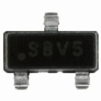
Package Information 4.1 TLV4946-2L Package Outline Figure 7 Marking of the TLV4946-2L and distance of the chip to the upper side Datasheet Year (y) = 0...9 Calendar Week (ww) = 01...52 14 TLV4946-2L Package Information Rev1.1, 2010-08-02 ...
Page 15
No solder function area Figure 8 PG-SSO-3-2 Package Outline Datasheet 0.8 x 45˚ ±0.1 7˚ 4.16 ±0.05 0.2 4.06 ±0.08 1.9 MAX. 0.6 MAX. 0.4 ±0. 1.27 ±0.25 1.27 ±0.25 12.7 ±1 ±0.4 12.7 ±0.3 ...
Page 16
... Published by Infineon Technologies AG ...