TLE4916-1K Infineon Technologies, TLE4916-1K Datasheet - Page 6
TLE4916-1K
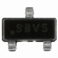
Manufacturer Part Number
TLE4916-1K
Description
IC HALL EFFECT SWITCH LP SC59-3
Manufacturer
Infineon Technologies
Type
Linear - Programmabler
Datasheet
1.TLE4916-1K.pdf
(16 pages)
Specifications of TLE4916-1K
Sensing Range
5mT Trip, -5mT Release
Voltage - Supply
2.4 V ~ 5 V
Current - Supply
4µA
Current - Output (max)
2mA
Output Type
Digital, Differential
Operating Temperature
-40°C ~ 125°C
Package / Case
TO-236-3, SC-59, SOT-23-3
Lead Free Status / RoHS Status
Lead free / RoHS Compliant
Features
-
Lead Free Status / Rohs Status
Lead free / RoHS Compliant
Available stocks
Company
Part Number
Manufacturer
Quantity
Price
Company:

Part Number:
TLE4916-1K
Manufacturer:
Kingston
Quantity:
12 000


2
2.1
The Low Power Hall IC Switch is comprised of a Hall probe, bias generator, compensation circuits, oscillator,
output latch and a n-channel open drain output transistor.
The bias generator provides currents for the Hall probe and the active circuits. Compensation circuits stabilize the
temperature behavior and reduce influence of technology variations.
The Active Error Compensation rejects offsets in signal stages and the influence of mechanical stress to the Hall
probe caused by molding and soldering processes and other thermal stresses in the package. This chopper
technique together with the threshold generator and the comparator ensure highly accurate magnetic switching
points.
Very low power consumption is achieved with a timing scheme controlled by an oscillator and a sequencer. This
circuitry activates the sensor for 50µs (typical operating time) sets the output state after sequential questioning of
the switch points and latches it with the beginning of the following standby phase (max. 120ms). In the standby
phase the average current is typically reduced to 3.5µA. Because of the long standby time compared to the
operating time the overall averaged current is only slightly higher than the standby current. The output transistor
can sink up to 1 mA with a maximal saturation voltage V
2.2
Figure 1
2.3
Table 1
Pin No.
1
2
3
Datasheet
1.5
Functional Description
General
Pin Configuration (top view)
Pin Configuration and Center of Sensitive Area
Pin Description
Pin Description
Symbol
V
Q
GND
1
S
± 0.15
SC59
3
2
Function
Supply voltage
Output
Ground
0.8
Sensitive Area
Center of
± 0.15
4
QSAT
Comment
Functional Description
Rev.1.0, 2010-02-23
TLE4916-1K
Related parts for TLE4916-1K
Image
Part Number
Description
Manufacturer
Datasheet
Request
R

Part Number:
Description:
Manufacturer:
Infineon Technologies AG
Datasheet:
Part Number:
Description:
Manufacturer:
Infineon Technologies AG
Datasheet:
Part Number:
Description:
Manufacturer:
Infineon Technologies AG
Datasheet:
Part Number:
Description:
Manufacturer:
Infineon Technologies AG
Datasheet:
Part Number:
Description:
Manufacturer:
Infineon Technologies AG
Datasheet:
Part Number:
Description:
Manufacturer:
Infineon Technologies AG
Datasheet:
Part Number:
Description:
Manufacturer:
Infineon Technologies AG
Datasheet:
Part Number:
Description:
16-bit microcontroller with 2x2 KByte RAM
Manufacturer:
Infineon Technologies AG
Datasheet:
Part Number:
Description:
NPN silicon RF transistor
Manufacturer:
Infineon Technologies AG
Datasheet:
Part Number:
Description:
NPN silicon RF transistor
Manufacturer:
Infineon Technologies AG
Datasheet:
Part Number:
Description:
NPN silicon RF transistor
Manufacturer:
Infineon Technologies AG
Datasheet:
Part Number:
Description:
NPN silicon RF transistor
Manufacturer:
Infineon Technologies AG
Datasheet:
Part Number:
Description:
Si-MMIC-amplifier in SIEGET 25-technologie
Manufacturer:
Infineon Technologies AG
Datasheet:
Part Number:
Description:
IGBT Power Module
Manufacturer:
Infineon Technologies AG
Datasheet:
Part Number:
Description:
IC for switching-mode power supplies
Manufacturer:
Infineon Technologies AG
Datasheet: