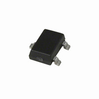
A1201LLHLT-T Allegro Microsystems Inc, A1201LLHLT-T Datasheet - Page 8

A1201LLHLT-T
Manufacturer Part Number
A1201LLHLT-T
Description
IC SW CONTINUOUS TIME BIPO SOT23
Manufacturer
Allegro Microsystems Inc
Type
Bipolar Latchr
Datasheet
1.A1203EUA-T.pdf
(13 pages)
Specifications of A1201LLHLT-T
Sensing Range
50G Trip, -50G Release
Voltage - Supply
3.8 V ~ 24 V
Current - Supply
7.5mA
Current - Output (max)
25mA
Output Type
Digital, Open Drain
Features
Regulated Voltage
Operating Temperature
-40°C ~ 150°C
Package / Case
SOT-23W
Lead Free Status / RoHS Status
Lead free / RoHS Compliant
Other names
620-1007-2
A1201
Bipolar Device Switching
The A1201 provides highly sensitive switching for applica-
tions using magnetic fields of alternating polarities, such as ring
magnets. There are three switching modes for bipolar devices,
referred to as latch, unipolar switch, and negative switch. Mode
is determined by the switchpoint characteristics of the individual
device. The characteristic hysteresis, B
difference in the relative magnetic strength and polarity of the
switchpoints of the device. (Note that, in the following descrip-
tions, a negative magnetic value indicates a north polarity field,
and a positive magnetic value indicates a south polarity field.
For a given value of magnetic strength, B
B
B = 0 indicates the absence of a magnetic field.)
Bipolar devices typically behave as latches. In this mode,
magnetic fields of opposite polarity and equivalent strengths
are needed to switch the output. When the magnetic fields are
removed (B 0) the device remains in the same state until a
magnetic field of the opposite polarity and of sufficient strength
causes it to switch. The hysteresis of latch mode behavior is
shown in panel A of figure 1.
Figure 1. Bipolar Device Output Switching Modes. These behaviors can be exhibited when using a circuit such as that shown in panel D. Panel A
displays the hysteresis when a device exhibits latch mode (note that the B
B
such as the A1201, can operate in any of the three modes.
HYS
X
indicate two fields of equal strength, but opposite polarity.
band is more positive than B = 0), and panel C shows negative switch behavior (the B
V+
0
B–
B
(A)
HYS
0
B+
V
V
CC
OUT(SAT)
HYS
X
, of the device, is the
, the values –B
Functional Description
V+
0
B– 0
X
and
B
(B)
HYS
HYS
Continuous-Time Bipolar Switch
band incorporates B= 0), panel B shows unipolar switch behavior (the
In contrast to latching, when a device exhibits unipolar switch-
ing, it only responds to a south magnetic field. The field must
be of sufficient strength, > B
the field is reduced beyond the B
back to the high state, as shown in panel B of figure 1. Devices
exhibiting negative switch behavior operate in a similar but
opposite manner. A north polarity field of sufficient strength,
> B
the result is that V
RP
V
S
, (more north than B
B+
V
V
CC
OUT(SAT)
HYS
band is more negative than B = 0). Bipolar devices,
OUT
switches high, as shown in panel C. When
A1201
V+
0
RP
115 Northeast Cutoff, Box 15036
Allegro MicroSystems, Inc.
Worcester, Massachusetts 01615-0036 (508) 853-5000
www.allegromicro.com
B–
VCC
GND
OP
(D)
) is required for operation, although
, for the device to operate. When
RP
VOUT
level, the device switches
B
(C)
HYS
R
L
0
Output
B+
V
V
CC
OUT(SAT)
8


