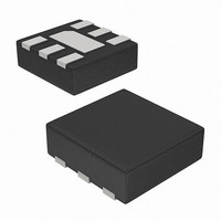
ISL29013IROZ-T7 Intersil, ISL29013IROZ-T7 Datasheet - Page 3

ISL29013IROZ-T7
Manufacturer Part Number
ISL29013IROZ-T7
Description
IC SENSOR LIGHT-DGTL I2C 6-ODFN
Manufacturer
Intersil
Datasheet
1.ISL29013IROZ-EVALZ.pdf
(15 pages)
Specifications of ISL29013IROZ-T7
Wavelength
540nm
Output Type
I²C™
Package / Case
6-ODFN
Rohs Compliant
Yes
Lead Free Status / RoHS Status
Lead free / RoHS Compliant
Other names
ISL29013IROZ-T7TR
Available stocks
Company
Part Number
Manufacturer
Quantity
Price
Company:
Part Number:
ISL29013IROZ-T7
Manufacturer:
Intersil
Quantity:
25
Pin Descriptions
Principles of Operation
Photodiodes
The ISL29013 contains two photodiode arrays which convert
light into current. One diode is sensitive to both visible and
infrared light, while the other one is only sensitive to infrared
light. Using the infrared portion of the light as baseline, the
visible light can be extracted. The spectral response vs
wavelength is shown in Figure 7 in the “Typical Performance
Curves” on page 12. After light is converted to current during
the light data process, the current output is converted to digital
by a single built-in integrating type signed15-bit Analog-to-
Digital Converter (ADC). An I
light intensity in counts.
The converter is a charge-balancing integrating type signed
15-bit ADC. The chosen method for conversion is best for
converting small current signals in the presence of an AC
periodic noise. A 100ms integration time, for instance, highly
rejects 50Hz and 60Hz power line noise simultaneously. See
“Integration Time or Conversion Time” on page 7 and “Noise
Rejection” on page 8.
The built-in ADC offers user flexibility in integration time or
conversion time. There are two timing modes: Internal Timing
Mode and External Timing Mode. In Internal Timing Mode,
integration time is determined by an internal dual speed
oscillator (f
the ADC. In External Timing Mode, integration time is
determined by the time between two consecutive I
Timing Mode commands. See External Timing Mode example.
A good balancing act of integration time and resolution
depending on the application is required for optimal results.
The ADC has four I
dynamically accommodate various lighting conditions. For
very dim conditions, the ADC can be configured at its lowest
range. For very bright conditions, the ADC can be configured
at its highest range.
PIN NUMBER
1
2
3
4
5
6
OSC
), and the n-bit (n = 4, 8, 12,16) counter inside
2
PIN NAME
C programmable range select to
REXT
GND
VDD
SCL
SDA
INT
2
C command reads the visible
3
Positive supply; connect this pin to a regulated 2.5V to 3.3V supply
Ground pin. The thermal pad is connected to the GND pin
External resistor pin for ADC reference; connect this pin to ground through a (nominal) 100kΩ resistor with
1% tolerance
Interrupt pin; LO for interrupt/alarming. The INT pin is an open drain.
I
I
2
2
C serial clock
C serial data
2
C External
ISL29013
The I
Interrupt Function
The active low interrupt pin is an open drain pull-down
configuration. The interrupt pin serves as an alarm or
monitoring function to determine whether the ambient light
exceeds the upper threshold or goes below the lower
threshold. The user can also configure the persistency of the
interrupt pin. This eliminates any false triggers such as noise
or sudden spikes in ambient light conditions. An unexpected
camera flash, for example, can be ignored by setting the
persistency to 8 integration cycles.
I
There are eight (8) 8-bit registers available inside the ISL29013.
The command and control registers define the operation of the
device. The command and control registers do not change until
the registers are overwritten. There are two 8-bit registers that
set the high and low interrupt thresholds. There are four 8-bit
data Read Only registers. Two bytes for the sensor reading and
another two bytes for the timer counts. The data registers
contain the ADC's latest digital output, and the number of clock
cycles in the previous integration period.
The ISL29013’s I
internally as 1000100. When 1000100x with x as R or W is
sent after the Start condition, this device compares the first
seven bits of this byte to its address and matches.
Figure 1 shows a sample one-byte read. Figure 2 shows a
sample one-byte write. Figure 3 shows a sync_I
diagram sample for externally controlled integration time.
The I
either the master or the slave can drive the SDA (data) line.
Figure 2 shows a sample write. Every I
with the master asserting a start condition (SDA falling while
SCL remains high). The following byte is driven by the
master, and includes the slave address and read/write bit.
The receiving device is responsible for pulling SDA low
during the acknowledgement period.
Every I
condition (SDA rising while SCL remains high).
For more information about the I
the Phillips
2
C Interface
2
C bus lines can pulled above VDD, 5.5V max.
2
DESCRIPTION
C bus master always drives the SCL (clock) line, while
2
C transaction ends with the master asserting a stop
®
I
2
C specification documents.
2
C interface slave address is hardwired
2
C standard, please consult
2
C transaction begins
September 2, 2008
2
C timing
FN6485.2


