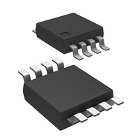
S-8130AACFN-MAET2G Seiko Instruments, S-8130AACFN-MAET2G Datasheet - Page 7

S-8130AACFN-MAET2G
Manufacturer Part Number
S-8130AACFN-MAET2G
Description
IC TEMP SWITCH W/LATCH 8-MSOP
Manufacturer
Seiko Instruments
Datasheet
1.S-8130AAAFN-MAAT2G.pdf
(13 pages)
Specifications of S-8130AACFN-MAET2G
Sensing Temperature
-40°C ~ 100°C
Output Type
Active High
Voltage - Supply
2.2 V ~ 10 V
Accuracy
±2.5°C
Package / Case
8-TSSOP, 8-MSOP (0.118", 3.00mm Width)
Maximum Operating Temperature
+ 100 C
Minimum Operating Temperature
- 40 C
Lead Free Status / RoHS Status
Lead free / RoHS Compliant
Rev.3.0
1. Basic operation
2. Voltage detection circuit with delay
Description of Operation
Noise Protection circuit
The noise protection circuit prevents malfunction of the temperature switch caused by noise.
T
•
•
S-8130AA series is a temperature switch which detects the temperature and sends a signal to an external
device. The users can select a combination of the parameters such as detection temperature and release
voltage.
The following is the case that the DET output is active high.
When the power voltage is turned on, the DET pin voltage goes to low since the flip-flop circuit in the
detection circuit is cleared by the delayed voltage detection circuit. Temperature detection then starts and
the DET pin is held low as long as the temperature is lower than the detection temperature.
temperature rises and when the temperature exceeds the detection temperature; longer than the time
defined by the capacitor connected to the CD1 pin, the DET pin goes to high. Once the over-temperature
is detected and the DET pin goes to high, the state is held by the flip-flop circuit. In order to release the
state the RESET pin voltage should be set to low by the external signal or the power voltage should be set
under the detection voltage of the built-in detector to reset the internal circuit.
Using the internal reference voltage and built-in temperature sensor, the accuracy of ±2.5°C in the
detection temperature is achieved.
The noise protection circuit starts charging the capacitor connected to the CD1 pin when the output of the
internal comparator enters active state due to an external noise or a rapid change in the power voltage. In
the normal operation the flip-flop circuit is set when the capacitor is charged to a certain voltage. But in the
noise triggered operation the comparator output goes back to inactive state and the CD1 pin voltage is
held low since the charging of the capacitor is insufficient. As a result the DET pin is held low and
malfunction does not occur.
Noise suppression time, T
and the capacitance C
The delay circuit in the voltage detector provides a delayed output signal to the RESET pin when the
power voltage V
power voltage V
The delay time, T
capacitance C
T
delay
noise
Noise suppression time coefficient (25°C): Typ. 6.4
Delay coefficient (25°C): Min. 4.3, Typ. 6.4, Max. 8.5
Layout the board wiring so that the current does not flow into or flow out of the CD2 pin to have correct
delay time since the impedance of the CD2 pin is high.
Capacitance of the external capacitor C
compared to the internal constant current. The difference occurs in delay time if the capacitor has leak
current. When the leak current is larger than the internal constant current, the voltage detection circuit
does not release reset.
(ms)=Delay coefficient × C
_00
(ms)=Noise suppression time coefficient × C
D2
DD
, and calculated by the following equation.
DD
delay
rises and exceeds the release voltage V
goes lower than the detection voltage, V
, is determined by the time constant consisting of internal constant current and the
D1
, and calculated by the following equation.
noise
, is determined by the time constant consisting of internal constant current
D2
(nF)
Seiko Instruments Inc.
D2
has no limitation as long as its leak current is negligible
D1
(nF)
TEMPERATURE SWITCH IC WITH LATCH
R
R
-V
. On the other hand no delay occurs when the
HYS
.
S-8130AA Series
The
7


