2N5114-E3 Vishay, 2N5114-E3 Datasheet - Page 4
2N5114-E3
Manufacturer Part Number
2N5114-E3
Description
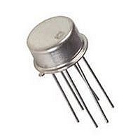
P CHANNEL JFET, 45V, TO-206AA
Manufacturer
Vishay
Specifications of 2N5114-E3
Breakdown Voltage Vbr
45V
Gate-source Cutoff Voltage Vgs(off) Max
10V
Power Dissipation Pd
500mW
Operating Temperature Range
-55°C To +200°C
No. Of Pins
3
Transistor Polarity
P Channel
Channel Type
P
Configuration
Single
Gate-source Voltage (max)
30V
Drain-gate Voltage (max)
30V
Operating Temperature (min)
-55C
Operating Temperature Classification
Military
Mounting
Through Hole
Pin Count
3
Continuous Drain Current Id
-90mA
Rohs Compliant
Yes
Lead Free Status / RoHS Status
Lead free / RoHS Compliant


2N4338/4339/4340/4341
Vishay Siliconix
www.vishay.com
4
TYPICAL CHARACTERISTICS (T
1500
1200
900
600
300
400
320
240
160
300
240
180
120
80
60
0
0
0
0
0
0
On-Resistance and Output Conductance
V
GS(off)
V
V
r
g
DS
vs. Gate-Source Cutoff Voltage
GS(off)
os
GS(off)
0.1
−1
4
= −0.7 V
r
@ I
@ V
DS
V
V
DS
DS
Output Characteristics
Output Characteristics
= −0.7 V
D
− Gate-Source Cutoff Voltage (V)
DS
− Drain-Source Voltage (V)
− Drain-Source Voltage (V)
= 100 mA, V
= 10 V, V
0.2
−2
8
GS
GS
V
= 0 V, f = 1 kHz
−0.5 V
g
GS
= 0 V
os
12
−3
0.3
= 0 V
V
A
GS
−4
16
−0.1 V
−0.2 V
−0.3 V
−0.4 V
−0.5 V
0.4
= 25_C UNLESS OTHERWISE NOTED)
−0.1 V
−0.2 V
−0.3 V
−0.4 V
= 0 V
0.5
20
−5
10
8
6
4
2
0
1.6
1.2
0.8
0.4
1.6
1.2
0.8
0.4
0.8
0.6
0.4
0.2
2
0
2
0
1
0
0
0.01
Common-Source Forward Transconductance
0
V
V
GS(off)
GS(off)
V
GS(off)
0.2
= −1.5 V
4
= −1.5 V
V
V
DS
DS
Output Characteristics
Output Characteristics
V
= −1.5 V
GS
I
− Drain-Source Voltage (V)
− Drain-Source Voltage (V)
D
vs. Drain Current
25_C
− Drain Current (mA)
= 0 V
0.4
8
−1.2 V
0.1
T
125_C
A
12
0.6
= −55_C
V
f = 1 kHz
DS
S-40990—Rev. F, 24-May-04
Document Number: 70240
= 10 V
V
GS
16
−0.3 V
−0.6 V
−0.9 V
−1.2 V
0.8
−0.3 V
−0.6 V
−0.9 V
= 0 V
1.0
20
1
Related parts for 2N5114-E3
Image
Part Number
Description
Manufacturer
Datasheet
Request
R

Part Number:
Description:
357-036-542-201 CARDEDGE 36POS DL .156 BLK LOPRO
Manufacturer:
Vishay
Datasheet:
Part Number:
Description:
357-036-542-201 CARDEDGE 36POS DL .156 BLK LOPRO
Manufacturer:
Vishay
Datasheet:
Part Number:
Description:
357-036-542-201 CARDEDGE 36POS DL .156 BLK LOPRO
Manufacturer:
Vishay
Datasheet:
Part Number:
Description:
357-036-542-201 CARDEDGE 36POS DL .156 BLK LOPRO
Manufacturer:
Vishay
Datasheet:
Part Number:
Description:
357-036-542-201 CARDEDGE 36POS DL .156 BLK LOPRO
Manufacturer:
Vishay
Datasheet:
Part Number:
Description:
357-036-542-201 CARDEDGE 36POS DL .156 BLK LOPRO
Manufacturer:
Vishay
Datasheet:
Part Number:
Description:
357-036-542-201 CARDEDGE 36POS DL .156 BLK LOPRO
Manufacturer:
Vishay
Datasheet:
Part Number:
Description:
357-036-542-201 CARDEDGE 36POS DL .156 BLK LOPRO
Manufacturer:
Vishay
Datasheet:
Part Number:
Description:
357-036-542-201 CARDEDGE 36POS DL .156 BLK LOPRO
Manufacturer:
Vishay
Datasheet:
Part Number:
Description:
357-036-542-201 CARDEDGE 36POS DL .156 BLK LOPRO
Manufacturer:
Vishay
Datasheet:
Part Number:
Description:
357-036-542-201 CARDEDGE 36POS DL .156 BLK LOPRO
Manufacturer:
Vishay
Datasheet:
Part Number:
Description:
357-036-542-201 CARDEDGE 36POS DL .156 BLK LOPRO
Manufacturer:
Vishay
Datasheet:
Part Number:
Description:
357-036-542-201 CARDEDGE 36POS DL .156 BLK LOPRO
Manufacturer:
Vishay
Datasheet:
Part Number:
Description:
357-036-542-201 CARDEDGE 36POS DL .156 BLK LOPRO
Manufacturer:
Vishay
Datasheet: