2N5911 Vishay, 2N5911 Datasheet - Page 2
2N5911
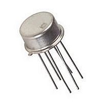
Manufacturer Part Number
2N5911
Description
MATCHED N CH JFET PAIR, -25V, TO-78
Manufacturer
Vishay
Specifications of 2N5911
Breakdown Voltage Vbr
-25V
Gate-source Cutoff Voltage Vgs(off) Max
-5V
Power Dissipation Pd
500mW
Operating Temperature Range
-55°C To +150°C
No. Of Pins
6
Continuous Drain Current Id
40mA
Channel Type
N
Configuration
Dual
Gate-source Voltage (max)
25V
Drain-gate Voltage (max)
-25V
Operating Temperature (min)
-55C
Operating Temperature (max)
150C
Operating Temperature Classification
Military
Mounting
Through Hole
Pin Count
7
Package Type
TO-78
Lead Free Status / RoHS Status
Contains lead / RoHS non-compliant


2N5911/5912
Vishay Siliconix
Notes
a.
b.
c.
www.vishay.com
8-2
Static
Gate-Source
Breakdown Voltage
Gate-Source Cutoff Voltage
Saturation Drain Current
Gate Reverse Current
Gate Operating Current
Gate-Source Voltage
Gate-Source
Forward Voltage
Dynamic
Common-Source
Forward Transconductance
Common-Source
Output Conductance
Common-Source
Forward Transconductance
Common-Source
Output Conductance
Common-Source
Input Capacitance
Common-Source Reverse
Transfer Capacitance
Equivalent Input
Noise Voltage
Noise Figure
Matching
Differential
Gate-Source Voltage
Gate-Source Voltage
Differential Change
with Temperature
Saturation Drain
Current Ratio
Transconductance Ratio
Differential Gate Current
Common Mode
Rejection Ratio
Typical values are for DESIGN AID ONLY, not guaranteed nor subject to production testing.
Pulse test: PW v300 ms duty cycle v3%.
This parameter not registered with JEDEC.
Parameter
c
c
b
D | V
| V
GS1
GS1
| I
Symbol
V
G1
V
I
CMRR
V
DT
I
(BR)GSS
DSS2
DSS1
GS(off)
I
I
– V
g
g
V
C
C
–I
DSS
GSS
GS(F)
g
g
– V
_
NF
g
g
I
e
fs1
fs2
GS
rss
G
os
os
iss
fs
fs
n
G2
GS2
GS2
|
|
|
V
DG
V
= 10 V, I
V
V
V
V
V
V
V
V
DG
V
V
V
V
V
V
V
Test Conditions
I
V
I
G
GS
DG
DG
DG
DG
DG
DG
DG
DG
G
DG
DS
DS
DG
DG
DS
DS
T
= 5 to 10 V, I
= –1 mA, V
= 1 mA, V
A
= –15 V, V
= 10 V, I
= 10 V, I
= 10 V, I
= 10 V, I
= 10 V, I
= 10 V, I
= 10 V, I
= 10 V, I
= 10 V, V
= 10 V, I
= 10 V, I
= 10 V, V
= 10 V, I
= 10 V, I
= 10 V, I
f = 100 MHz
= –55 to 125_C
f = 10 kHz
f = 1 MHz
f = 1 kHz
f = 1 kHz
D
= 5 mA, T
D
D
D
D
D
D
D
D
G
D
D
DS
D
D
DS
GS
GS
DS
= 5 mA
= 5 mA
= 5 mA
= 5 mA
= 5 mA
= 5 mA
= 5 mA
= 5 mA
= 5 mA
= 5 mA
R
= 5 mA
= 5 mA
= 1 nA
D
T
T
= 0 V
= 0 V
G
A
A
= 0 V
= 0 V
= 5 mA
= 0 V
A
= 100 kW
= 150_C
= 125_C
= 125_C
Typ
0.005
–3.5
–0.3
–1.5
0.98
0.98
–35
0.7
5.8
0.1
15
–1
–2
–1
70
90
15
85
6
3
1
4
4
a
Min
–0.3
0.95
0.95
–25
–1
7
5
5
2N5911
Max
–100
–250
–100
–100
100
150
1.2
–5
40
–4
10
10
20
10
20
20
5
1
1
1
Limits
S-04031—Rev. D, 04-Jun-01
Min
–0.3
0.95
0.95
–25
Document Number: 70255
–1
7
5
5
2N5912
Max
–100
–250
–100
–100
100
150
1.2
–5
40
–4
10
10
20
15
40
20
5
1
1
1
mV/_C
Unit
mA
mS
mS
mV
nV
pA
nA
pA
nA
mS
mS
pF
dB
nA
dB
V
V
V
Hz
NZF
Related parts for 2N5911
Image
Part Number
Description
Manufacturer
Datasheet
Request
R

Part Number:
Description:
357-036-542-201 CARDEDGE 36POS DL .156 BLK LOPRO
Manufacturer:
Vishay
Datasheet:
Part Number:
Description:
357-036-542-201 CARDEDGE 36POS DL .156 BLK LOPRO
Manufacturer:
Vishay
Datasheet:
Part Number:
Description:
357-036-542-201 CARDEDGE 36POS DL .156 BLK LOPRO
Manufacturer:
Vishay
Datasheet:
Part Number:
Description:
357-036-542-201 CARDEDGE 36POS DL .156 BLK LOPRO
Manufacturer:
Vishay
Datasheet:
Part Number:
Description:
357-036-542-201 CARDEDGE 36POS DL .156 BLK LOPRO
Manufacturer:
Vishay
Datasheet:
Part Number:
Description:
357-036-542-201 CARDEDGE 36POS DL .156 BLK LOPRO
Manufacturer:
Vishay
Datasheet:
Part Number:
Description:
357-036-542-201 CARDEDGE 36POS DL .156 BLK LOPRO
Manufacturer:
Vishay
Datasheet:
Part Number:
Description:
357-036-542-201 CARDEDGE 36POS DL .156 BLK LOPRO
Manufacturer:
Vishay
Datasheet:
Part Number:
Description:
357-036-542-201 CARDEDGE 36POS DL .156 BLK LOPRO
Manufacturer:
Vishay
Datasheet:
Part Number:
Description:
357-036-542-201 CARDEDGE 36POS DL .156 BLK LOPRO
Manufacturer:
Vishay
Datasheet:
Part Number:
Description:
357-036-542-201 CARDEDGE 36POS DL .156 BLK LOPRO
Manufacturer:
Vishay
Datasheet:
Part Number:
Description:
357-036-542-201 CARDEDGE 36POS DL .156 BLK LOPRO
Manufacturer:
Vishay
Datasheet:
Part Number:
Description:
357-036-542-201 CARDEDGE 36POS DL .156 BLK LOPRO
Manufacturer:
Vishay
Datasheet:
Part Number:
Description:
357-036-542-201 CARDEDGE 36POS DL .156 BLK LOPRO
Manufacturer:
Vishay
Datasheet:
Part Number:
Description:
357-036-542-201 CARDEDGE 36POS DL .156 BLK LOPRO
Manufacturer:
Vishay
Datasheet: