2N5461-E3 Vishay, 2N5461-E3 Datasheet - Page 3
2N5461-E3
Manufacturer Part Number
2N5461-E3
Description
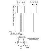
TRANSISTOR,JFET,P-Channel,9mA I(DSS),TO-92
Manufacturer
Vishay
Datasheet
1.2N5462.pdf
(5 pages)
Specifications of 2N5461-E3
Breakdown Voltage Vbr
40V
Gate-source Cutoff Voltage Vgs(off) Max
7.5V
Power Dissipation Pd
350mW
Operating Temperature Range
-55°C To +150°C
No. Of Pins
3
Continuous Drain Current Id
-9mA
Rohs Compliant
Yes
Lead Free Status / RoHS Status
Lead free / RoHS Compliant


Document Number: 70262
S-04030—Rev. D, 04-Jun-01
–1.6
–1.2
–0.8
–0.4
–0.5
–0.4
–0.3
–0.2
–0.1
–20
–16
–12
–8
–4
–2
0
0
0
V
0
0
0
GS(off)
V
V
GS
GS(off)
0.2 V
Drain Current and Transconductance
= 0 V
= 1.5 V
V
vs. Gate-Source Cutoff Voltage
–0.2
GS(off)
= 1.5 V
–4
2
V
V
g
fs
DS
DS
Output Characteristics
Output Characteristics
– Gate-Source Cutoff Voltage (V)
g
I
f = 1 kHz
DSS
– Drain-Source Voltage (V)
– Drain-Source Voltage (V)
fs
@ V
@ V
–0.4
–8
4
DS
DS
= –15 V, V
= –15 V, V
–0.6
I
–12
DSS
6
0.4 V
GS
GS
= 0 V
V
= 0 V
GS
–0.8
–16
8
= 0 V
0.2 V
0.4 V
0.6 V
0.8 V
1.0 V
0.8 V
1.0 V
1.2 V
0.6 V
–20
–1
10
_
5
2.5
0
1000
–1.6
–1.2
–0.8
–0.4
800
600
400
200
–10
–8
–6
–4
–2
–2
0
0
0
0
0
0
On-Resistance and Output Conductance
V
V
GS(off)
GS(off)
V
vs. Gate-Source Cutoff Voltage
GS(off)
–0.2
–4
= 3 V
2
= 3 V
r
V
V
DS
DS
DS
Output Characteristics
Output Characteristics
– Gate-Source Cutoff Voltage (V)
r
g
f = 1 kHz
DS
os
– Drain-Source Voltage (V)
– Drain-Source Voltage (V)
@ I
@ V
–0.4
2N/SST5460 Series
–8
4
D
DS
= –100 mA, V
= –15 V, V
0.5 V
–0.6
g
–12
Vishay Siliconix
os
6
V
GS
GS
GS
= 0 V
= 0 V
= 0 V
V
GS
–0.8
–16
8
= 0 V
0.5 V
1.0 V
1.5 V
2.0 V
1.0 V
1.5 V
2.0 V
2.5 V
www.vishay.com
–20
10
–1
100
80
60
40
20
0
9-3
Related parts for 2N5461-E3
Image
Part Number
Description
Manufacturer
Datasheet
Request
R

Part Number:
Description:
357-036-542-201 CARDEDGE 36POS DL .156 BLK LOPRO
Manufacturer:
Vishay
Datasheet:
Part Number:
Description:
357-036-542-201 CARDEDGE 36POS DL .156 BLK LOPRO
Manufacturer:
Vishay
Datasheet:
Part Number:
Description:
357-036-542-201 CARDEDGE 36POS DL .156 BLK LOPRO
Manufacturer:
Vishay
Datasheet:
Part Number:
Description:
357-036-542-201 CARDEDGE 36POS DL .156 BLK LOPRO
Manufacturer:
Vishay
Datasheet:
Part Number:
Description:
357-036-542-201 CARDEDGE 36POS DL .156 BLK LOPRO
Manufacturer:
Vishay
Datasheet:
Part Number:
Description:
357-036-542-201 CARDEDGE 36POS DL .156 BLK LOPRO
Manufacturer:
Vishay
Datasheet:
Part Number:
Description:
357-036-542-201 CARDEDGE 36POS DL .156 BLK LOPRO
Manufacturer:
Vishay
Datasheet:
Part Number:
Description:
357-036-542-201 CARDEDGE 36POS DL .156 BLK LOPRO
Manufacturer:
Vishay
Datasheet:
Part Number:
Description:
357-036-542-201 CARDEDGE 36POS DL .156 BLK LOPRO
Manufacturer:
Vishay
Datasheet:
Part Number:
Description:
357-036-542-201 CARDEDGE 36POS DL .156 BLK LOPRO
Manufacturer:
Vishay
Datasheet:
Part Number:
Description:
357-036-542-201 CARDEDGE 36POS DL .156 BLK LOPRO
Manufacturer:
Vishay
Datasheet:
Part Number:
Description:
357-036-542-201 CARDEDGE 36POS DL .156 BLK LOPRO
Manufacturer:
Vishay
Datasheet:
Part Number:
Description:
357-036-542-201 CARDEDGE 36POS DL .156 BLK LOPRO
Manufacturer:
Vishay
Datasheet:
Part Number:
Description:
357-036-542-201 CARDEDGE 36POS DL .156 BLK LOPRO
Manufacturer:
Vishay
Datasheet: