SI8435DB-T1-E1 Vishay, SI8435DB-T1-E1 Datasheet - Page 7
SI8435DB-T1-E1
Manufacturer Part Number
SI8435DB-T1-E1
Description
P CH MOSFET, -20V, 10A, MICRO FOOT
Manufacturer
Vishay
Series
TrenchFET®r
Specifications of SI8435DB-T1-E1
Transistor Polarity
P Channel
Continuous Drain Current Id
-10A
Drain Source Voltage Vds
-20V
On Resistance Rds(on)
75mohm
Rds(on) Test Voltage Vgs
5V
Threshold Voltage Vgs Typ
-1V
Fet Type
MOSFET P-Channel, Metal Oxide
Fet Feature
Standard
Rds On (max) @ Id, Vgs
41 mOhm @ 1A, 4.5V
Drain To Source Voltage (vdss)
20V
Current - Continuous Drain (id) @ 25° C
10A
Vgs(th) (max) @ Id
1V @ 250µA
Gate Charge (qg) @ Vgs
35nC @ 5V
Input Capacitance (ciss) @ Vds
1600pF @ 10V
Power - Max
6.25W
Mounting Type
Surface Mount
Package / Case
4-MICRO FOOT®CSP
Configuration
Single Dual Drain
Resistance Drain-source Rds (on)
0.041 Ohms
Drain-source Breakdown Voltage
- 20 V
Gate-source Breakdown Voltage
+/- 5 V
Continuous Drain Current
6.72 A
Power Dissipation
2.78 W
Maximum Operating Temperature
+ 150 C
Mounting Style
SMD/SMT
Minimum Operating Temperature
- 55 C
Lead Free Status / RoHS Status
Lead free / RoHS Compliant
Lead Free Status / RoHS Status
Lead free / RoHS Compliant, Lead free / RoHS Compliant
Other names
SI8435DB-T1-E1TR


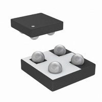
PACKAGE OUTLINE
MICRO FOOT: 4-BUMP (2 x 2, 0.8 mm PITCH)
Notes (Unless Otherwise Specified):
1. Laser mark on the silicon die back, coated with a thin metal.
2. Bumps are Sn/Ag/Cu.
3. Non-solder mask defined copper landing pad.
4. The flat side of wafers is oriented at the bottom.
Notes:
a. Use millimeters as the primary measurement.
Vishay Siliconix maintains worldwide manufacturing capability. Products may be manufactured at one of several qualified locations. Reliability data for Silicon
Technology and Package Reliability represent a composite of all qualified locations. For related documents such as package/tape drawings, part marking, and
reliability data, see http://www.vishay.com/ppg?73559.
Document Number: 73559
S-82119-Rev. D, 08-Sep-08
Dim.
A
A
A
D
b
E
e
S
1
2
e
Recommended Land
Mark on Backside of Die
X X X
8435
e
0.600
0.260
0.340
0.370
1.520
1.520
0.750
0.370
Min.
Millimeters
Note 3
Solder Mask ∅ ~ 0.40
4 x ∅ 0.30 ~ 0.31
a
b Diameter
A
0.650
0.290
0.360
0.410
1.600
1.600
0.850
0.380
Max.
A
A
2
1
E
Silicon
D
e
0.0236
0.0102
0.0134
0.0146
0.0598
0.0598
0.0295
0.0146
Min.
S
Inches
Bump Note 2
Vishay Siliconix
S
e
Si8435DB
www.vishay.com
0.0256
0.0114
0.0142
0.0161
0.0630
0.0630
0.0335
0.0150
Max.
7
Related parts for SI8435DB-T1-E1
Image
Part Number
Description
Manufacturer
Datasheet
Request
R

Part Number:
Description:
P-channel 1.5-v G-s Mosfet
Manufacturer:
Vishay
Datasheet:

Part Number:
Description:
IC ISOLATOR 3CH 2.5KV 16SOIC
Manufacturer:
Silicon Laboratories Inc

Part Number:
Description:
TRIPLE-CHANNEL DIGITAL ISOLATOR
Manufacturer:
SILABS [Silicon Laboratories]
Datasheet:
Part Number:
Description:
357-036-542-201 CARDEDGE 36POS DL .156 BLK LOPRO
Manufacturer:
Vishay
Datasheet:
Part Number:
Description:
357-036-542-201 CARDEDGE 36POS DL .156 BLK LOPRO
Manufacturer:
Vishay
Datasheet:
Part Number:
Description:
357-036-542-201 CARDEDGE 36POS DL .156 BLK LOPRO
Manufacturer:
Vishay
Datasheet:
Part Number:
Description:
357-036-542-201 CARDEDGE 36POS DL .156 BLK LOPRO
Manufacturer:
Vishay
Datasheet:
Part Number:
Description:
357-036-542-201 CARDEDGE 36POS DL .156 BLK LOPRO
Manufacturer:
Vishay
Datasheet:
Part Number:
Description:
357-036-542-201 CARDEDGE 36POS DL .156 BLK LOPRO
Manufacturer:
Vishay
Datasheet:
Part Number:
Description:
357-036-542-201 CARDEDGE 36POS DL .156 BLK LOPRO
Manufacturer:
Vishay
Datasheet:
Part Number:
Description:
357-036-542-201 CARDEDGE 36POS DL .156 BLK LOPRO
Manufacturer:
Vishay
Datasheet:
Part Number:
Description:
357-036-542-201 CARDEDGE 36POS DL .156 BLK LOPRO
Manufacturer:
Vishay
Datasheet:
Part Number:
Description:
357-036-542-201 CARDEDGE 36POS DL .156 BLK LOPRO
Manufacturer:
Vishay
Datasheet:
Part Number:
Description:
357-036-542-201 CARDEDGE 36POS DL .156 BLK LOPRO
Manufacturer:
Vishay
Datasheet:
Part Number:
Description:
357-036-542-201 CARDEDGE 36POS DL .156 BLK LOPRO
Manufacturer:
Vishay
Datasheet: