AMMP-6233-TR2G Avago Technologies US Inc., AMMP-6233-TR2G Datasheet - Page 2
AMMP-6233-TR2G
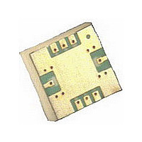
Manufacturer Part Number
AMMP-6233-TR2G
Description
LNA, MMIC, 18 - 31 GHz, Pkg
Manufacturer
Avago Technologies US Inc.
Datasheet
1.AMMP-6233-TR2G.pdf
(8 pages)
Specifications of AMMP-6233-TR2G
Current - Supply
65mA
Frequency
18GHz ~ 32GHz
Gain
23.2dB
Noise Figure
2.6dB
P1db
8dBm
Package / Case
8-SMD
Rf Type
VSAT, DBS
Test Frequency
18GHz
Voltage - Supply
3 V ~ 5 V
Number Of Channels
1
Frequency (max)
32GHz
Power Supply Requirement
Single
Single Supply Voltage (typ)
3V
Single Supply Voltage (max)
5V
Package Type
SMD
Dual Supply Voltage (min)
Not RequiredV
Dual Supply Voltage (typ)
Not RequiredV
Dual Supply Voltage (max)
Not RequiredV
Supply Current
90@3VmA
Pin Count
8
Mounting
Surface Mount
Lead Free Status / RoHS Status
Lead free / RoHS Compliant
Lead Free Status / RoHS Status
Lead free / RoHS Compliant
Available stocks
Company
Part Number
Manufacturer
Quantity
Price

Part Number:
AMMP-6233-TR2G
Manufacturer:
AVAGO/安华高
Quantity:
20 000


Absolute Maximum Ratings
Notes:
1. Operation in excess of any of these conditions may result in per-
AMMP-6233 RF Specifications
TA= 25°C, Vdd=3.0 V, Idd= 65 mA, Zin=Zo=50 Ω
Notes:
4. Small/Large -signal data measured in a fully de-embedded test fixture form TA = 25°C.
5. Specifications are derived from measurements in a 50 Ω test environment. Aspects of the amplifier performance may be improved over a nar-
6. All tested parameters guaranteed with measurement accuracy +/-0.5dB for NF and +/-1dB for gain at 18GHz, 26GHz and +/-1.5dB for gain at
Sym
Vd
Id
Pin
Tch
Tstg
Tmax Maximum Assembly Temp
Symbol
Freq
Gain
NF
Rlin
Rlout
Iso
P1dB
OIP3
manent damage to this device. The absolute maximum ratings for
Vd, Id and Pin were determined at an ambient temperature of 25°C
unless noted otherwise.
rower bandwidth by application of additional conjugate, linearity, or low noise (Gopt) matching.
29GHz.
Parameters/Condition
Drain to Ground Voltage
Drain Current
RF CW Input Power Max
Max channel temperature
Storage temperature
Parameters and Test Conditions
Operational Frequency
RF Small Signal Gain
Noise Figure into 50Ω
Input Return Loss
Output Return Loss
Isolation
Output Power at 1dB gain compression
Output Third Order Intercept Point
(1)
(4,5,6)
Unit
V
mA
dBm
C
C
C
Max
5.5
100
10
+150
-65 +150
260 for 20s
Freq
18GHz
26GHz
29GHz
18GHz
26GHz
29GHz
DC Specifications/ Physical Properties
Notes:
2. Ambient operational temperature TA=25°C unless noted
3. Channel-to-backside Thermal Resistance (Tchannel = 34°C) as mea-
Sym
Idd
Vd
qjc
sured using infrared microscopy. Thermal Resistance at backside
temp. (Tb) = 25°C calculated from measured data.
Parameter and Test
Condition
Drain Supply Cur-
rent under any RF
power drive and temp.
(V
Drain Supply Voltage
Thermal Resistance
dd
=3.0 V)
Units
GHz
dB
dB
dB
dB
dB
dB
dB
dB
dB
dBm
dBm
Min.
18
19
20.8
20
-10
-13
-45
8
18
(3)
Unit
mA
V
C/W
Typ.
23.2
24.4
23.6
2.6
2.2
2.6
(2)
Min
40
Typ
65
3
27
Max.
32
3.6
3.2
3.5
Max
90
5
Related parts for AMMP-6233-TR2G
Image
Part Number
Description
Manufacturer
Datasheet
Request
R

Part Number:
Description:
IC MMIC LNA 18GHZ-31GHZ 8SMD
Manufacturer:
Avago Technologies US Inc.
Datasheet:

Part Number:
Description:
IC MMIC LNA 18GHZ-31GHZ 8SMD
Manufacturer:
Avago Technologies US Inc.
Datasheet:

Part Number:
Description:
IC AMP GP HI PWR 6-20GHZ 8-SMD
Manufacturer:
Avago Technologies US Inc.
Datasheet:

Part Number:
Description:
IC AMP GP HI PWR 6-20GHZ 8-SMD
Manufacturer:
Avago Technologies US Inc.
Datasheet:
Part Number:
Description:
IC MMIC AMP HGA 6-20GHZ 8SMD
Manufacturer:
Avago Technologies US Inc.
Datasheet:

Part Number:
Description:
IC MMIC AMP HGA 6-20GHZ 8SMD
Manufacturer:
Avago Technologies US Inc.
Datasheet:
Part Number:
Description:
IC MMIC LOW NOISE 6-20GHZ 8-SMD
Manufacturer:
Avago Technologies US Inc.
Datasheet:
Part Number:
Description:
IC AMP GP HI PWR 6-20GHZ 8-SMD
Manufacturer:
Avago Technologies US Inc.
Datasheet:

Part Number:
Description:
6-20 GHz High Gain Amp In SMT Pkg
Manufacturer:
Avago Technologies US Inc.
Datasheet:

Part Number:
Description:
Power Amp, MMIC, 6-18GHz Pkg
Manufacturer:
Avago Technologies US Inc.
Datasheet:

Part Number:
Description:
OPTOCOUPLER GATE DRV 2A 16-SOIC
Manufacturer:
Avago Technologies US Inc.
Datasheet:
Part Number:
Description:
OPTOCOUPLER 2CH 2.5A 16-SOIC
Manufacturer:
Avago Technologies US Inc.
Datasheet:

Part Number:
Description:
OPTOCOUPLER GATE DRV 0.4A 16SOIC
Manufacturer:
Avago Technologies US Inc.
Datasheet:

Part Number:
Description:
OPTOCOUPLER 2.0A 250KHZ 8-DIP
Manufacturer:
Avago Technologies US Inc.
Datasheet:

Part Number:
Description:
OPTOCOUPLER 2.0A 250KHZ GW 8-SMD
Manufacturer:
Avago Technologies US Inc.
Datasheet: