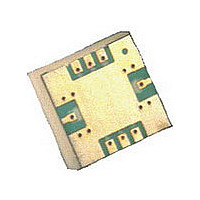
AMMP-6522-BLKG Avago Technologies US Inc., AMMP-6522-BLKG Datasheet
AMMP-6522-BLKG
Specifications of AMMP-6522-BLKG


Related parts for AMMP-6522-BLKG


AMMP-6522-BLKG Summary of contents
Page 1
... GHz GaAs MMIC LNA/IRM Receiver in SMT Package Data Sheet Description Avago’s AMMP-6522 is an easy-to-use broadband inte- grated receiver in a surface mount package. The MMIC includes a 3-stage LNA to provide gain amplification and a gate-pumped image-reject mixer for frequency translation. The overall receiver performs Single Side Band down-conversion in the GHz RF signal range. The LO and RF are matched to 50 Ω ...
Page 2
Absolute Maximum Ratings Symbol Parameter and Test Condition Vdd Drain to Ground Voltage Vg Gate to Ground Voltage Idd Drain Current Ig Gate Current Pin RF CW Input Power Max Tch Max channel temperature Tstg Storage temperature Tmax Maximum ...
Page 3
... AMMP-6522 Typical Performance (T = 25°C, Vdd = 4 V, Idd = 75 mA Power = +15 dBm unless noted -10 - FREQUENCY (GHz) Figure 1. Receiver conversion gain 0 -10 -20 - FREQUENCY (GHz) Figure 3. Return loss at RF & LO ports - POWER (dBm) Figure 5. Conv gain vs. LO power ( GHz FREQUENCY (GHz) Figure 7. LSB conversion gain at two IF frequencies ...
Page 4
... AMMP-6522 Typical Performance (cont 25°C, Vdd = 4 V, Idd = 75 mA unless noted - FREQUENCY (GHz) Figure 9. Conversion gain over FREQUENCY (GHz) Figure 11. Receiver conversion gain over Vdd 0 -10 -20 - FREQUENCY (GHz) Figure 13. Return loss at RF over temperature 0 25°C -40°C 85°C -10 -20 ...
Page 5
... The image rejection performance is dependent on the selection of the IF quadrature hybrid. The performance of the IF hybrid as well as the phase balance and VSWR of the interface to the AMMP-6522 will affect the overall front end performance. There is minimal performance degradation if Vdd is lowered raised lower current is required, then Vdd = 3 V will provide considerably similar RF performance ...
Page 6
LSB USB Figure 18. Theory of harmonic rejection Figure 19. Evaluation/test board VDD RF Figure 20. Simplified LNA with IRM Receiver Schematic (the IF quadrature hybrid is external to the circuit) 6 cos (LO - IF) ...
Page 7
... Recommended SMT Attachment for 5x5 Package The AMMP Packaged Devices are compatible with high volume surface mount PCB assembly processes. The PCB material and mounting pattern, as defined in the data sheet, optimizes RF performance and is strong- ly recommended. An electronic drawing of the land pattern is available upon request from Agilent Sales & ...
Page 8
... TIME (SECONDS) Figure 22. Suggested lead-free Reflow Profile for SnAgCu solder paste AMMP-6522 Part Number Ordering Information Part Number Devices per Container Container AMMP-6522-BLKG 10 AMMP-6522-TR1G 100 AMMP-6522-TR2G 500 8 A properly designed solder screen or stencil is required to ensure optimum amount of solder paste is deposited onto the PCB pads ...
Page 9
... R 0.50 TYP. 1.75 ± 0.10 5.50 ± 0.05 Ø1.50 (MIN.) 8.00 ± 0. PITCH: WIDTH: Notes Pitches cumulative tolerance is ± 0.2 Mm. 3. Dimensions are in millimeters (mm). AMMP AMMP XXXX XXXX www.avagotech.com 0.114 (2.90) 0.018 (0.46) 0.014 (0.365 0.012 (0.30 0.028 (0.70) 0.93 (2.36) ...