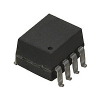
HCNR200#300 Avago Technologies US Inc., HCNR200#300 Datasheet - Page 9

HCNR200#300
Manufacturer Part Number
HCNR200#300
Description
Photodiode-Output Optocoupler,1-CHANNEL,5kV ISOLATION,DIP
Manufacturer
Avago Technologies US Inc.
Datasheet
1.HCNR201-500E.pdf
(19 pages)
Specifications of HCNR200#300
Number Of Channels
1
Input Type
DC
Voltage - Isolation
5000Vrms
Current Transfer Ratio (min)
0.25% @ 10mA
Current Transfer Ratio (max)
0.75% @ 10mA
Current - Dc Forward (if)
25mA
Output Type
Linear Photovoltaic
Mounting Type
Surface Mount, Gull Wing
Package / Case
8-SMD Gull Wing
Output Device
Linear Photovoltaic
Number Of Elements
1
Reverse Breakdown Voltage
2.5V
Forward Voltage
1.95V
Forward Current
25mA
Collector-emitter Voltage
Not RequiredV
Package Type
PDIP W SMD
Collector Current (dc) (max)
Not RequiredA
Isolation Voltage
5000Vrms
Power Dissipation
60mW
Collector-emitter Saturation Voltage
Not RequiredV
Current Transfer Ratio
Not Required%
Pin Count
8
Mounting
Surface Mount
Operating Temp Range
-40C to 85C
Operating Temperature Classification
Industrial
Lead Free Status / RoHS Status
Contains lead / RoHS non-compliant
Voltage - Output
-
Current - Output / Channel
-
Vce Saturation (max)
-
Lead Free Status / Rohs Status
Not Compliant
Available stocks
Company
Part Number
Manufacturer
Quantity
Price
AC Electrical Specifications
T
LED Bandwidth
Application Circuit Bandwidth:
High Speed
High Precision
Application Circuit: IMRR
High Speed
Package Characteristics
T
Input‑Output
Momentary‑Withstand
Voltage*
Resistance
(Input‑Output)
Capacitance
(Input‑Output)
*The Input‑Output Momentary Withstand Voltage is a dielectric voltage rating that should not be interpreted as an input‑output continuous
voltage rating. For the continuous voltage rating refer to the VDE 0884 Insulation Characteristics Table (if applicable), your equipment level safety
specification, or Application Note 1074, “Optocoupler Input‑Output Endurance Voltage. ”
Notes:
1. K
2. BEST FIT DC NONLINEARITY (NL
3. ENDS FIT DC NONLINEARITY (NL
4. Device considered a two‑terminal device: Pins 1, 2, 3, and 4 shorted together and pins 5, 6, 7, and 8 shorted together.
5. In accordance with UL 1577, each optocoupler is proof tested by applying an insulation test voltage of ≥6000 V rms for ≥1 second (leakage
6. Specific performance will depend on circuit topology and components.
7. IMRR is defined as the ratio of the signal gain (with signal applied to V
9
A
A
= 25°C unless otherwise specified.
= 25°C unless otherwise specified.
Parameter
Parameter
mately equal to I
a graph of I
the best fit line, expressed as a percentage of the full scale output.
the 50 µA data point on the graph of I
detection current limit, I
IEC/EN/DIN EN 60747‑5‑2 Insulation Characteris‑tics Table (for Option #050 only).
common and the signal applied between the input and output commons) at 60 Hz, expressed in dB.
3
is calculated from the slope of the best fit line of I
PD2
vs. I
PD2
PD1
/I
with eleven equally distributed data points from 5 nA to 50 µA. I
PD1
at I
I‑O
of 5 µA max.). This test is performed before the 100% production test for partial discharge (method b) shown in the
F
= 10 mA.
BF
EF
) is the maximum deviation expressed as a percentage of the full scale output of a “best fit” straight line from
) is the maximum deviation expressed as a percentage of full scale output of a straight line from the 5 nA to
Symbol
V
R
C
PD2
ISO
I‑O
I‑O
vs. I
PD1
Symbol
f ‑3dB
.
Device
PD2
vs. I
Device
PD1
5000
with eleven equally distributed data points from 5 nA to 50 µA. This is approxi‑
Min.
10
10
12
11
IN
Min.
of Figure 16) to the isolation mode gain (with V
Typ.
10
0.4
13
Typ.
1.5
10
95
9
Max.
0.6
PD2
error to best fit line is the deviation below and above
Max.
V rms
Units
pF
Ω
Units
MHz
MHz
kHz
dB
Test
RH ≤50%,
t = 1 min.
V
T
V
f = 1 MHz
A
O
IO
= 100°C,
= 500 VDC
= 500 VDC
Conditions
Test
I
freq = 60 Hz
F
Conditions
= 10 mA
IN
connected to input
Fig.
Fig.
16
17
16
Note
Note
6, 7
4, 5
6
6
4
4
4


