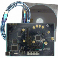
AD9910/PCBZ Analog Devices Inc, AD9910/PCBZ Datasheet - Page 37
AD9910/PCBZ
Manufacturer Part Number
AD9910/PCBZ
Description
Direct Digital Synthesis Evaluation Board
Manufacturer
Analog Devices Inc
Series
AgileRF™r
Specifications of AD9910/PCBZ
Silicon Manufacturer
Analog Devices
Application Sub Type
Direct Digital Synthesizer
Kit Application Type
Clock & Timing
Silicon Core Number
AD9910
Kit Contents
Board
Design Resources
Synchronizing Multiple AD9910 1 GSPS Direct Digital Synthesizers (CN0121)
Main Purpose
Timing, Direct Digital Synthesis (DDS)
Embedded
No
Utilized Ic / Part
AD9910
Primary Attributes
14-Bit DAC, 32-Bit Tuning Word Width
Secondary Attributes
1GHz, Graphical User Interface
Lead Free Status / RoHS Status
Lead free / RoHS Compliant
Lead Free Status / RoHS Status
Lead free / RoHS Compliant, Lead free / RoHS Compliant
Other names
Q3335404


The gray bar across the top indicates the time interval over
which the designated profile is in effect. The circled numbers
indicate specific events as follows:
Event 1—An I/O update registers the internal profile control bits
(in Control Function Register 1) as 0010. The RAM_SWP_OVR
pin is set to Logic 0. The state machine is initialized to the
waveform start address of RAM Profile 0 and begins increment-
ing through the address range for RAM Profile 0 at intervals of
Δt
Event 2—The state machine reaches the waveform end address
of RAM Profile 0, and the RAM_SWP_OVR pin generates a
positive pulse spanning two DDS clock cycles.
Event 3—Having reached the waveform end address of RAM
Profile 0, the next expiration of the internal timer causes the
state machine to advance to RAM Profile 1. The state machine
is initialized to the waveform start address of RAM Profile 1
and begins incrementing through the address range for RAM
Profile 1 at intervals of Δt
0
(as specified by the address step rate for RAM Profile 0).
RAM_SWP_OVER
I/O_UPDATE
RAM PROFILE
ADDRESS
RAM
1
.
1
WAVEFORM START ADDRESS 2
WAVEFORM START ADDRESS 0
WAVEFORM START ADDRESS 1
WAVEFORM END ADDRESS 2
WAVEFORM END ADDRESS 1
WAVEFORM END ADDRESS 0
Δ
t
0
0
Figure 44. Internal Profile Control Timing Diagram (Burst)
1
2
3
Δ
t
1
1
1
Rev. C | Page 37 of 64
4
5
Event 4—The state machine reaches the waveform end address
of RAM Profile 1, and the RAM_SWP_OVR pin generates a
positive pulse spanning two DDS clock cycles.
Event 5—Having reached the waveform end address of RAM
Profile 1, the next expiration of the internal timer causes the
state machine to advance to RAM Profile 2. The state machine
initializes to the waveform start address of RAM Profile 2 and
begins incrementing through the address range for RAM
Profile 2 at intervals of Δt
Event 6—The state machine reaches the waveform end address of
RAM Profile 2, and the RAM_SWP_OVR pin generates a positive
pulse spanning two DDS clock cycles.
Event 7—Having reached the waveform end address of RAM
Profile 2, the next expiration of the internal timer causes the
state machine to halt and marks completion of the burst
waveform generation process.
Δ
t
2
2
1
2
.
6
7
AD9910
Related parts for AD9910/PCBZ
Image
Part Number
Description
Manufacturer
Datasheet
Request
R


Part Number:
Description:
±1.7g Dual-Axis IMEMS Accelerometer Evaluation Board
Manufacturer:
Analog Devices Inc
Datasheet:

Part Number:
Description:
Inertial Sensor Evaluation System
Manufacturer:
Analog Devices Inc
Datasheet:
Part Number:
Description:
Manufacturer:
Analog Devices Inc
Datasheet:
Part Number:
Description:
Manufacturer:
Analog Devices Inc
Datasheet:
Part Number:
Description:
Manufacturer:
Analog Devices Inc
Datasheet:
Part Number:
Description:
Manufacturer:
Analog Devices Inc
Datasheet:
Part Number:
Description:
Manufacturer:
Analog Devices Inc
Datasheet:
Part Number:
Description:
Manufacturer:
Analog Devices Inc
Datasheet:
Part Number:
Description:
Manufacturer:
Analog Devices Inc
Datasheet:
Part Number:
Description:
Manufacturer:
Analog Devices Inc
Datasheet:
Part Number:
Description:
Manufacturer:
Analog Devices Inc
Datasheet:
Part Number:
Description:
Manufacturer:
Analog Devices Inc
Datasheet: