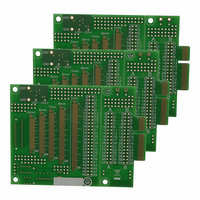
AC164139 Microchip Technology, AC164139 Datasheet - Page 275

AC164139
Manufacturer Part Number
AC164139
Description
Graphics Display Prototype Board Graphics
Manufacturer
Microchip Technology
Specifications of AC164139
Main Purpose
LCD Development
Embedded
No
Utilized Ic / Part
PICtail™ Plus Board
Lead Free Status / RoHS Status
Lead free / RoHS Compliant
Secondary Attributes
-
Primary Attributes
-
Lead Free Status / RoHS Status
Lead free / RoHS Compliant
Available stocks
Company
Part Number
Manufacturer
Quantity
Price
Company:
Part Number:
AC164139
Manufacturer:
Microchip Technology
Quantity:
135
- Current page: 275 of 408
- Download datasheet (4Mb)
REGISTER 19-1:
2010 Microchip Technology Inc.
bit 15
bit 7
Legend:
R = Readable bit
-n = Value at POR
bit 15
bit 14
bit 13
bit 12-11
bit 10
bit 9-8
bit 7-6
bit 5
bit 4
bit 3
bit 2
bit 1-0
PMPEN
R/W-0
R/W-0
CSF1
PMPEN: Parallel Master Port Enable bit
1 = EPMP is enabled
0 = EPMP is disabled
Unimplemented: Read as ‘0’
PSIDL: Stop in Idle Mode bit
1 = Discontinue module operation when device enters Idle mode
0 = Continue module operation in Idle mode
ADRMUX<1:0>: Address/Data Multiplexing Selection bits
11 = Lower address bits are multiplexed with data bits using 3 address phases
10 = Lower address bits are multiplexed with data bits using 2 address phases
01 = Lower address bits are multiplexed with data bits using 1 address phase
00 = Address and data appear on separate pins
Unimplemented: Read as ‘0’
MODE<1:0>: Parallel Port Mode Select bits
11 = Master mode
10 = Enhanced PSP; pins used are PMRD, PMWR, PMCS, PMD<7:0> and PMA<1:0>
01 = Buffered PSP; pins used are PMRD, PMWR, PMCS and PMD<7:0>
00 = Legacy Parallel Slave Port; PMRD, PMWR, PMCS and PMD<7:0> pins are used
CSF<1:0>: Chip Select Function bits
11 = Reserved
10 = PMA<15> used for Chip Select 2, PMA<14> used for Chip Select 1
01 = PMA<15> used for Chip Select 2, PMCS1 used for Chip Select 1
00 = PMCS2 used for Chip Select 2, PMCS1 used for Chip Select 1
ALP: Address Latch Polarity bit
1 = Active-high (PMALL, PMALH and PMALU)
0 = Active-low (PMALL, PMALH and PMALU)
ALMODE: Address Latch Strobe Mode bit
1 = Enable “smart” address strobes (each address phase is only present if the current access would
0 = Disable “smart” address strobes
Unimplemented: Read as ‘0’
BUSKEEP: Bus Keeper bit
1 = Data bus keeps its last value when not actively being driven
0 = Data bus is in high-impedance state when not actively being driven
IRQM<1:0>: Interrupt Request Mode bits
11 = Interrupt generated when Read Buffer 3 is read or Write Buffer 3 is written (Buffered PSP mode),
10 = Reserved
01 = Interrupt generated at the end of a read/write cycle
00 = No interrupt is generated
R/W-0
CSF0
U-0
cause a different address in the latch than the previous address)
—
or on a read or write operation when PMA<1:0> = 11 (Addressable PSP mode only)
PMCON1: EPMP CONTROL REGISTER 1
W = Writable bit
‘1’ = Bit is set
R/W-0
PSIDL
R/W-0
ALP
ADRMUX1
ALMODE
PIC24FJ256DA210 FAMILY
R/W-0
R/W-0
U = Unimplemented bit, read as ‘0’
‘0’ = Bit is cleared
ADRMUX0
R/W-0
U-0
—
BUSKEEP
R/W-0
U-0
—
x = Bit is unknown
MODE1
IRQM1
R/W-0
R/W-0
DS39969B-page 275
MODE0
IRQM0
R/W-0
R/W-0
bit 8
bit 0
Related parts for AC164139
Image
Part Number
Description
Manufacturer
Datasheet
Request
R

Part Number:
Description:
Manufacturer:
Microchip Technology Inc.
Datasheet:

Part Number:
Description:
Manufacturer:
Microchip Technology Inc.
Datasheet:

Part Number:
Description:
Manufacturer:
Microchip Technology Inc.
Datasheet:

Part Number:
Description:
Manufacturer:
Microchip Technology Inc.
Datasheet:

Part Number:
Description:
Manufacturer:
Microchip Technology Inc.
Datasheet:

Part Number:
Description:
Manufacturer:
Microchip Technology Inc.
Datasheet:

Part Number:
Description:
Manufacturer:
Microchip Technology Inc.
Datasheet:

Part Number:
Description:
Manufacturer:
Microchip Technology Inc.
Datasheet:


