CDK5571 Cirrus Logic Inc, CDK5571 Datasheet - Page 14
CDK5571
Manufacturer Part Number
CDK5571
Description
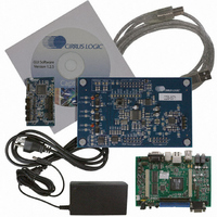
KIT - CDB557 W/ Capture Plus II System
Manufacturer
Cirrus Logic Inc
Series
CapturePLUS™IIr
Datasheets
1.CS5571-ISZ.pdf
(34 pages)
2.CDB5571.pdf
(26 pages)
3.CDK5571.pdf
(1 pages)
4.CDK5571.pdf
(42 pages)
Specifications of CDK5571
Number Of Adc's
1
Number Of Bits
16
Sampling Rate (per Second)
100k
Data Interface
Serial
Inputs Per Adc
2 Single
Input Range
2.4 ~ 4.2 V
Voltage Supply Source
Dual ±
Operating Temperature
-40°C ~ 85°C
Utilized Ic / Part
CS5571
Lead Free Status / RoHS Status
Contains lead / RoHS non-compliant
Other names
598-1279
CDK5571-1
CDK5571-1


3/25/08
CS5571
10:56
Once a conversion is completed and RDY falls, RDY will return high when all the bits of the data word are
emptied from the serial port or if the conversion data is not read and CS is held low, RDY will go high two
MCLK cycles before the end of conversion. RDY will fall at the end of the next conversion when new data
is put into the port register.
See
Serial Port
on page 26 for information about reading conversion data.
Conversion performance can be affected by several factors. These include the choice of clock source for
the chip, the timing of CONV, the setting of the DITHER function, and the choice of the serial port mode.
The converter can be operated from an internal oscillator. This clock source has greater jitter than an
external crystal-based clock. Jitter may not be an issue when measuring DC signals, or very-low-fre-
quency AC signals, but can become an issue for higher frequency AC signals. For maximum performance
when digitizing AC signals, a low-jitter MCLK should be used.
To achieve the highest resolution when measuring a DC signal with a single conversion the DITHER func-
tion should be off. If averaging is to be performed with multiple conversions of a DC signal, DITHER
should be on. To maximize performance, the CONV pin should be held low in the continuous conversion
state to perform multiple conversions, or CONV should occur synchronous to MCLK, falling when MCLK
falls.
If the converter is operated at maximum throughput, the SSC serial port mode is less likely to cause in-
terference to measurements as the SCLK output is synchronized to the MCLK. Alternately, any interfer-
ence due to serial port clocking can also be minimized if data is read in the SEC serial port mode when a
conversion is not in progress.
3.2 Clock
The CS5571 can be operated from its internal oscillator or from an external master clock. The state of
MCLK determines which clock source will be used. If MCLK is tied low, the internal oscillator will start and
be used as the clock source for the converter. If an external CMOS-compatible clock is input into MCLK,
the converter will power down the internal oscillator and use the external clock. If the MCLK pin is held
high, the internal oscillator will be held in the stopped state. The MCLK input can be held high to delete
clock cycles to aid in synchronizing multiple converters in different phase relationships.
The internal oscillator can be used if the signals to be measured are essentially DC. The internal oscillator
exhibits jitter at about 500 picoseconds rms. If the CS5571 is used to digitize AC signals, an external
low-jitter clock source should be used.
If the internal oscillator is used as the clock for the CS5571, the maximum conversion rate will be dictated
by the oscillator frequency.
If driven from an external MCLK source, the fast rise and fall times of the MCLK signal can result in clock
coupling from the internal bond wire of the IC to the analog input. Adding a 50 ohm resistor on the external
MCLK source significantly reduces this effect.
14
DS768PP1
Related parts for CDK5571
Image
Part Number
Description
Manufacturer
Datasheet
Request
R

Part Number:
Description:
Development Kit
Manufacturer:
Cirrus Logic Inc
Datasheet:
Part Number:
Description:
Development Kit
Manufacturer:
Cirrus Logic Inc
Datasheet:


Part Number:
Description:
High-efficiency PFC + Fluorescent Lamp Driver Reference Design
Manufacturer:
Cirrus Logic Inc
Datasheet:
Part Number:
Description:
Development Kit
Manufacturer:
Cirrus Logic Inc
Datasheet:
Part Number:
Description:
Development Kit
Manufacturer:
Cirrus Logic Inc
Datasheet:

Part Number:
Description:
Development Kit
Manufacturer:
Cirrus Logic Inc
Datasheet:
Part Number:
Description:
Development Kit
Manufacturer:
Cirrus Logic Inc
Datasheet:
Part Number:
Description:
Development Kit
Manufacturer:
Cirrus Logic Inc
Datasheet:
Part Number:
Description:
Development Kit
Manufacturer:
Cirrus Logic Inc
Datasheet:

Part Number:
Description:
EVALUATION BOARD FOR CS8427
Manufacturer:
Cirrus Logic Inc
Datasheet:

Part Number:
Description:
BOARD EVAL FOR CS8416 RCVR
Manufacturer:
Cirrus Logic Inc
Datasheet:

Part Number:
Description:
EVALUATION BOARD FOR CS8420
Manufacturer:
Cirrus Logic Inc
Datasheet:

Part Number:
Description:
KIT DEVELOPMENT EP9315 ARM9
Manufacturer:
Cirrus Logic Inc
Datasheet:

Part Number:
Description:
KIT DEVELOPMENT EP9302 ARM9
Manufacturer:
Cirrus Logic Inc
Datasheet: