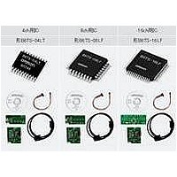
B6TS-04LT Omron, B6TS-04LT Datasheet - Page 20

B6TS-04LT
Manufacturer Part Number
B6TS-04LT
Description
Capacitance Touch Sensors Sensing IC
Manufacturer
Omron
Series
-r
Type
Capacitiver
Specifications of B6TS-04LT
Sensitivity
-
Response Time
-
Interface
SPI
Channel Inputs
4 Key
Voltage - Supply
3 V ~ 5 V
Actuator Type
-
Package / Case
20-LSSOP (0.173", 4.40mm Width)
Lead Free Status / RoHS Status
Lead free / RoHS Compliant
8.4
8.5
8.6
Designation
V
V
I
I
I
Designation
-
-
-
Designation
t
t
t
t
t
T
T
t
T
T
t
t
t
T
T
T
c(SCK)
w(SCKH)
w(SCKL)
r(SCK)
f(SCK)
d(SO)
h(SI)
w(BD)
w(CD)
IH
IL
CC
su(SCS)
h(SCS)
d(SCS)
su(SI)
w(CHG)
su(SETUP)
w(RESET)
OH
OL
Electrical characteristics (2) [Vdd=3V]
Electrical characteristics (3)
Necessary timing conditions
Note 1: Unless otherwise specified, Vdd = 3.0-3.3V, Topr = -20-85°C.
Note 1: Unless otherwise specified, Vdd = 3.0-5.5V, Topr = -20-85°C
Note 2: The period following receipt of the EEPROM write command in setup mode until the data write
finishes.
Note 1: Unless otherwise specified, Vdd = 3.0-5.5V, Topr = 25°C.
Note 2: This is the time period when the condition that CHG pulse width is at its minimum in the serial
communication mode of normal measurement mode is set.
(CHG pin function is set to output at the end of every measurement [CHG bit = 0 with MODE
command]) and the sleep time is set to zero [SLP command value = 0]).
Note 3: The delay time for the mode shift between normal measurement mode and setup mode.
Item
High output voltage
Low output voltage
High input current
Low input current
Supply current
Item
Number of times of
EEPROM write
EEPROM write time
EEPROM data retention
period
Item
Serial communication clock cycle time
Serial communication clock high pulse width
Serial communication clock low pulse width
Serial communication clock rise time
Serial communication clock fall time
Serial communication chip select setup time
Serial communication chip select hold time
Serial communication output delay time
Serial communication chip select delay time
Serial communication input setup time
Serial communication input hold time
Serial communication byte to byte interval
Serial communication command reception
interval
CHG pulse width
Mode shift delay time
Reset pulse width
Condition
I
I
V
V
Normal measurement
mode
During sleep
OH
OL
I
I
=3V
=0V
=1mA
=-1mA
Condition
T
V
(Note 2)
T
OPR
OPR
dd
=5V, T
=0∼60°C
=55°C
OPR
=25°C
Condition
(Note 2)
(Note 3)
Minimum
Minimum
V
10000
dd
20
-0.5
Rated value
Rated value
Standard
Standard
Minimum
4.8
0.4
0.3
320
320
100
280
130
500
0.4
0.4
15
90
50
Rated value
Maximum
Maximum
Maximum
V
0.5
-4
4
dd
280
320
0.6
0.6
95
1
1
Unit
V
V
µA
µA
mA
mA
Unit
Times
S
Years
Unit
µS
t
t
µS
µS
nS
nS
nS
nS
nS
nS
µS
µS
µS
µS
µS
c(SCK)
c(SCK)


