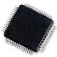
HV633PG-G Supertex, HV633PG-G Datasheet - Page 10

HV633PG-G
Manufacturer Part Number
HV633PG-G
Description
Display Drivers 32-Channel 256 Gray- Shade High Voltage
Manufacturer
Supertex
Datasheet
1.HV633PG-G.pdf
(13 pages)
Specifications of HV633PG-G
Driver Type
EL Lamp Drivers
Operating Supply Voltage
- 0.5 V to + 7.5 V
Maximum Operating Temperature
+ 125 C
Mounting Style
SMD/SMT
Package / Case
PQFP-64
Supply Current
20 mA
Lead Free Status / RoHS Status
Lead free / RoHS Compliant
Pin Descriptions
* Analog VDD and digital VDD may be connected seperately for better noise immunity.
Pin #
10
12
13
14
15
16
17
18
19
20
21
22
23
24
25
26
27
28
11
1
2
3
4
5
6
7
8
9
Supertex inc.
SC (shift clock)
VDD (analog)*
Function
HV
HV
HV
HV
HV
HV
HV
HVGND
LVGND
HV
HV
HV
HV
HV
HV
HV
HV
HV
VCTL
RCTL
VPP
CSI
DIR
NC
NC
VR
OUT
OUT
OUT
OUT
OUT
OUT
OUT
OUT
OUT
OUT
OUT
OUT
OUT
OUT
OUT
OUT
10
12
13
14
15
16
11
1
2
3
4
5
6
7
8
9
●
Description
High-voltage outputs
This is ground for the high-voltage (output) section. HVGND and LVGND should be
connected together externally.
High voltage ramp input for charging the output stage hold capacitors (CH). This input
can be linear or non-linear as desired.
This input biases the output source followers.
No connect.
Low-voltage analog supply voltage.
Input pin for the chip select pulse (when DIR is high). Output pin for the chip select
pulse (when DIR is low).
No connect.
Voltage supply pin to prevent output voltage from being affected by its adjacent outputs
(V
output voltage variation to less than ±0.2V of delta voltage between high voltage
outputs of the same level at all gray levels.
Current sense resistor to ground to prevent output voltage from being affected by its
adjacent outputs (R
Triggers data on both rising and falling edges. This implies that the data rate is always
twice the clock rate (data rate = 20MHz if clock rate = 10MHz).
This is ground for the logic section. HVGND and LVGND should be connected together
externally.
When this pin is connected to VDD, input data is shifted in ascending order, i.e.,
corresponding to HV
in descending order, i.e., corresponding to HV
1235 Bordeaux Drive, Sunnyvale, CA 94089
CTL
= 2.0V for a particular panel). The combination of V
CTL
OUT
= 56KΩ for a particular panel). See VCTL function above.
1 to HV
10
OUT
32. When connected to LVGND, input data is shifted
●
Tel: 408-222-8888
OUT
32 to HV
●
OUT
CTL
www.supertex.com
1.
and R
CTL
will reduce the
HV633


