HV633PG-G Supertex, HV633PG-G Datasheet - Page 9
HV633PG-G
Manufacturer Part Number
HV633PG-G
Description
Display Drivers 32-Channel 256 Gray- Shade High Voltage
Manufacturer
Supertex
Datasheet
1.HV633PG-G.pdf
(13 pages)
Specifications of HV633PG-G
Driver Type
EL Lamp Drivers
Operating Supply Voltage
- 0.5 V to + 7.5 V
Maximum Operating Temperature
+ 125 C
Mounting Style
SMD/SMT
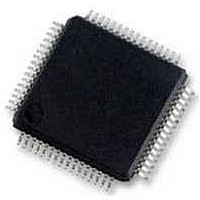
Package / Case
PQFP-64
Supply Current
20 mA
Lead Free Status / RoHS Status
Lead free / RoHS Compliant


Theory of Operation
The HV633 has two primary functions:
Since the device was developed initially for flat panel dis-
plays, the operation will be described in terms that pertain
to that technology. As shown by the Typical Panel Connec-
tions, several HV633 packages are mounted at the top and
bottom of a display panel. Data exists on a 7-bit bus (adja-
cent PC board traces) at top and bottom. The D1 through
D7 inputs of each chip take data from the bus when either a
CSI or CSO pulse is present at the chip. These pulses there-
fore act as a combination CHIP SELECT and LOCATION
STROBE. Because of the way the chip HV
quenced, data on the bus at the bottom of the display panel
will be entered into the left-most chip as HV
etc. up to HV
DIR = High.
Loading Data from Data Bus
Here is the full data-entry sequence:
1) The microcontroller puts data on the bus (7 bits)
2) To enter the data into the 32 sets of 7 latches on the first
chip, the shift clock rises. This positive transition is combined
with the CSI pulse and is generated only once to strobe the
data into the first set of latches. (These latches eventually
send data to the HV
the shift clock falls, and this negative transition is combined
with the CSI pulse, which is now propagated internally, to
strobe the new data into the next set of 7 latches (which will
end up as HV
twice the shift clock rate.
3) When the last set of 7 latches in the first chip has been
loaded (HV
chip 2. The exit pin is called CSO and the chip 2 entry pin is
CSI. For chips at the top of the panel things are reversed:
DIR is low, entry pins are CSO and exit pins are CSI, be-
cause the data-into-latches sequence is in descending or-
der, HV
4) The buses may of course be separate, and data can be
strobed in on an interleaved basis, etc., but those complica-
tions will be left to systems designers.
1) Loading data from the data bus and,
2) Gray-shade conversion(converting latched data to out-
put voltages).
OUT
32 down to HV
OUT
Supertex inc.
OUT
OUT
32), the CSI pulse leaves chip 1 and enters
32. The CSI pulse will accomplish this with
2). This internal CSI pulse therefore runs at
OUT
1). The data on the bus then changes,
OUT
1.
●
1235 Bordeaux Drive, Sunnyvale, CA 94089
OUT
OUT
pins are se-
1, HV
OUT
2,
9
When data has been loaded into all 32 outputs of all chips
(top and bottom of the display panel), the load count pin is
pulsed. On its rising transition, all output levels are reset to
zero and all the data in the input latches is transferred to a
like number of comparator latches, (thus leaving the data
latches ready to receive new data during the following op-
erations). After the transfer, the load countpin is brought low.
This transition begins the events that convert the binary data
into a gray-shade level.
Gray-shade Conversion
1) The COUNT CLOCK is started. An external signal is ap-
plied to the COUNT CLOCK pin, causing the counter on
each chip to increment from binary 000 0000 to 111 1111 (0
to 127).
2) At the same time, the V
charging transistors, causing the HOLD CAPACITOR (CH)
on each output to experience a rise in voltage.
3) The logic control compares the count in the comparator
latch to the count clock. The gate voltage of Q1 and the out-
put voltage HV
4) Once V
pixels will be at the final value. (See Gray Scale Voltage.)
Output Voltage Variation
The output voltage of the HV633 is determined by the logic
and the ramp voltage V
age may be coupled to an unacceptable level due to its
adjacent outputs through the panel. In order to solve this
problem, internal logic (refer to Output Stage Detail) is in-
tegrated in the IC to minimize the effect. Two external pins
VCTL and RCTL allow the feasibility to control the current
flowing through Q2. The VCTL pin is connected to a voltage
source and the RCTL pin is connected to ground through a
resistor (2.0V and 56KΩ are used for a particular panel). The
internal bias circuit will drive the resistor to a voltage level
that is equal to the VCTL voltage at steady state through an
operational amplifier. The current flowing through Q1 and Q2
will be limited to VCTL/RCTL. This combination of VCTL and
RCTL will reduce the output voltage variation to less than
±0.2V of delta voltage for each gray shade, independent of
its adjacent output voltages.
R
●
has reached the maximum voltage, then all the
Tel: 408-222-8888
OUT
will ramp up at the same rate as VR.
R
. It is possible that the output volt-
R
voltage is applied to all chips, via
●
www.supertex.com
HV633
Related parts for HV633PG-G
Image
Part Number
Description
Manufacturer
Datasheet
Request
R

Part Number:
Description:
32-channel 128-level Amplitude Gray-shade Display Column Driver
Manufacturer:
Supertex, Inc.
Datasheet:
Part Number:
Description:
32-channel Serial To Parallel Converter With High Voltage Push-pull Outputs - Supertex, Inc
Manufacturer:
Supertex, Inc.
Datasheet:
