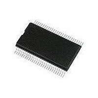
PCF8579TD NXP Semiconductors, PCF8579TD Datasheet - Page 20

PCF8579TD
Manufacturer Part Number
PCF8579TD
Description
LCD Drivers LCD DRVR DOT MATRIX
Manufacturer
NXP Semiconductors
Datasheet
1.PCF8579T1112.pdf
(41 pages)
Specifications of PCF8579TD
Maximum Clock Frequency
10 KHz
Operating Supply Voltage
2.5 V to 6 V
Maximum Power Dissipation
400 mW
Package / Case
VSO-56
Maximum Supply Current
20 uA
Lead Free Status / RoHS Status
Lead free / RoHS Compliant
Other names
PCF8579T/1,112
NXP Semiconductors
PCF8579_5
Product data sheet
8.9 RAM access
There are three RAM-access modes:
These modes are specified by the bits G[1:0] of the RAM-access command. The
RAM-access command controls the order in which data is written to or read from the RAM
(see
To store RAM data, the user specifies the location into which the first byte will be loaded
(see
Subsequent data bytes will be written or read according to the chosen RAM-access mode.
Device subaddresses are automatically incremented between devices until the last device
is reached. If the last device has subaddress 15, further display data transfers will lead to
a wrap-around of the subaddress to 0.
Fig 15. RAM addressing scheme
•
•
•
•
•
•
Character
Half-graphic
Full-graphic
Device subaddress (specified by the device-select command)
RAM X-address (specified by the bits X[5:0] of the load-X-address command)
RAM bank (specified by the bits Y[1:0] of the RAM-access command)
Figure
Figure
MSB
LSB
17).
16):
1 byte
Rev. 05 — 11 May 2009
0
LCD column driver for dot matrix graphic displays
X address
X max
PCF8579
© NXP B.V. 2009. All rights reserved.
Y max
0
Y address
001aaj920
20 of 41


