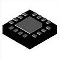
MAX17149ETE+ Maxim Integrated Products, MAX17149ETE+ Datasheet - Page 8

MAX17149ETE+
Manufacturer Part Number
MAX17149ETE+
Description
LED Drivers 6-String WLED Driver
Manufacturer
Maxim Integrated Products
Datasheet
1.MAX17129ETE.pdf
(20 pages)
Specifications of MAX17149ETE+
Operating Supply Voltage
3 V to 26 V
Maximum Supply Current
4 mA
Maximum Power Dissipation
1176 mW
Maximum Operating Temperature
+ 85 C
Mounting Style
SMD/SMT
Package / Case
TQFN-16
Minimum Operating Temperature
- 40 C
Lead Free Status / RoHS Status
Lead free / RoHS Compliant
Low-Cost, 6-String WLED Drivers with
Quick-PWM Step-Up Converter
8
PIN
1
2
3
4
5
6
7
8
9
NAME
PGND
FSEL
OVP
BRT
V
FB1
FB2
LX
IN
CC
PWM Signal Input. This PWM signal controls the LED brightness by turning the LED current sources on
or off.
Internal LDO Output. V
Connect a minimum 1FF capacitor from V
exceeds its UVLO threshold. See the Input Supply Voltage Configuration and UVLO section for supply
configurations for the ICs.
Supply Input. Connect IN to the system input supply voltage and bypass IN to GND with a minimum
0.1FF ceramic capacitor. The ICs are disabled if V
devices can extend the operating range down to 3.0V if IN and V
Supply Voltage Configuration and UVLO section.
Step-Up Converter Switching Frequency Selection Input. Connect to V
500kHz, or connect to GND to set 1MHz.
Step-Up Regulator Switching Node. Connect inductor and output diode here and minimize trace area
for lowest EMI.
Power Ground
Boost Output Voltage-Sensing Input. This voltage is used for overvoltage protection.
Current-Balancer Output. LED string cathode connection. FB1 is the open-drain output of an internal
regulator, which controls current through FB1. FB1 can sink up to 45mA. If unused, connect FB1 to
GND or leave high impedance.
Current-Balancer Output. LED string cathode connection. FB2 is the open-drain output of an internal
regulator, which controls current through FB2. FB2 can sink up to 45mA. If unused, connect FB2 to
GND or leave high impedance.
TOP VIEW
GND
ISET
FB6
EN
CC
13
14
15
16
provides bias supply to the devices. V
+
12
1
3mm × 3mm
THIN QFN
MAX17129
MAX17149
11
2
10
CC
3
to GND. All power outputs are disabled until V
FUNCTION
EP
9
4
IN
8
7
6
5
falls below its UVLO (5.625V typ) threshold. The
FB1
OVP
PGND
LX
CC
CC
is generated by internal LDO.
are tied together. See the Input
CC
Pin Configuration
with a 10kω resistor to set
Pin Description
CC


