LDS8621002-T2-960/960 Leadis Technology, LDS8621002-T2-960/960 Datasheet - Page 3

LDS8621002-T2-960/960
Manufacturer Part Number
LDS8621002-T2-960/960
Description
LED Drivers 200mA Dual Output w/ PWM intereface
Manufacturer
Leadis Technology
Datasheet
1.LDS8621002-T2-960960.pdf
(8 pages)
Specifications of LDS8621002-T2-960/960
Low Level Output Current
0 mA
High Level Output Current
192 mA
Operating Supply Voltage
2.7 V to 5.5 V
Maximum Operating Temperature
+ 85 C
Mounting Style
SMD/SMT
Package / Case
TQFN-16
Minimum Operating Temperature
- 45 C
Lead Free Status / RoHS Status
Lead free / RoHS Compliant
LDS8621
PIN DESCRIPTION
PIN FUNCTION
V
ceramic bypass capacitor is required between the Vin
pin and ground near the device. The operating input
voltage range is from 2.5V to 5.5V. Whenever the
input supply falls below the under-voltage threshold
(1.8V), all the LED channels are disabled and the
device enters shutdown mode.
V
the LED anodes. A small 1
capacitor is required between the V
ground near the device.
GND is the ground reference for the charge pump.
The pin must be connected to the ground plane on
the PCB.
C1+, C1- are connected to each side of the ceramic
bucket capacitor C1
C2+, C2- are connected to each side of the ceramic
bucket capacitor C2
© 2008 Leadis Technology
Characteristics subject to change without notice
15, 16
IN
OUT
Pin #
4 - 6
PAD
10
11
12
13
14
is the supply pin for the charge pump. A small 1
1
2
3
7
8
9
is the charge pump output that is connected to
PWM2
PWM1
Name
LEDA
LEDB
GND
V
PAD
C1+
C2+
C1-
C2-
NC
NC
V
OUT
IN
No connect
LED A cathode terminal
LED B cathode terminal
No connect
Charge pump output connected to the LED anodes
Charge pump input, connect to battery or supply
Bucket capacitor 1 Positive terminal
Bucket capacitor 1 Negative terminal
Bucket capacitor 2 Positive terminal
Bucket capacitor 2 Negative terminal
LEDB PWM brightness control
LEDA PWM brightness control
Ground Reference, Connect both pins to GND
Connect to GND on the PCB
LEADIS TECHNOLOGY CONFIDENTIAL
μ
F ceramic bypass
PRELIMINARY
OUT
Function
pin and
μ
F
3
LEDA and LEDB provide the internal regulated
current source for each of the LED cathodes.
These pins enter high-impedance zero current
state whenever the device is in shutdown mode.
PAD is the exposed pad underneath the package.
For best thermal performance, the pad should be
soldered to the PCB and connected to the ground
plane
PWM1, PWM2 are the enable and PWM LED
brightness control logic inputs. Guaranteed levels
of logic high and logic low are set at 1.3 V and 0.4
V respectively. When any of PWM pins is taken
high, the device becomes enabled with maximum
LED current at associated LED. To place the
LDS8621 into zero current mode, both PWM pins
must be held low for more than 30 ms.
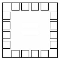
Top view: TQFN 16-lead 3 X 3 mm
Doc. No. 8621DS, Rev. 0.2


