EVALA5970D STMicroelectronics, EVALA5970D Datasheet - Page 9
EVALA5970D
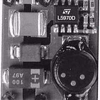
Manufacturer Part Number
EVALA5970D
Description
Power Management Modules & Development Tools EVAL BOARD A5970D Auto Grade
Manufacturer
STMicroelectronics
Type
DC/DC Switching Converters, Regulators & Controllersr
Datasheet
1.EVALA5970D.pdf
(31 pages)
Specifications of EVALA5970D
Input Voltage
4.4 V to 36 V
Output Voltage
1.235 V to 35 V
Board Size
23 mm x 20 mm
Product
Power Management Modules
Supply Current
1 A
Dimensions
23 mm x 20 mm
For Use With/related Products
AN1330
Lead Free Status / RoHS Status
Lead free / RoHS Compliant


AN1330
2.6
reference (1.235 V), while the inverting input (FB) is connected to the external divider or
directly to the output voltage. The output (COMP) is connected to the external compensation
network. The uncompensated error amplifier has the following characteristics:
Table 2.
The error amplifier output is compared with the oscillator sawtooth to perform PWM control.
PWM comparator and power stage
This block compares the oscillator sawtooth and the error amplifier output signals
generating the PWM signal for the driving stage.
The power stage is a highly critical block, as it functions to guarantee a correct turn ON and
turn OFF of the PDMOS. The turn ON of the power element, or more accurately, the rise
time of the current at turn ON, is a very critical parameter. At a first approach, it appears that
the faster the rise time, the lower the turn ON losses. However, there is a limit introduced by
the recovery time of the recirculation diode.
In fact, when the current of the power element is equal to the inductor current, the diode
turns OFF and the drain of the power is able to go high. But during its recovery time, the
diode can be considered a high value capacitor and this produces a very high peak current,
responsible of many problems:
●
●
●
●
The fall time of the current during the turn OFF is also critical, as it produces voltage spikes
(due to the parasitic elements of the board) that increase the voltage drop across the
PDMOS.
In order to minimize these problems, a new driving circuit topology has been used and the
block diagram is shown in
turn the power switch ON and OFF, based on the PDMOS and the gate clamp status.
This circuitry allows the power switch to be turned OFF and ON quickly and addresses the
freewheeling diode recovery time problem. The gate clamp is necessary to avoid that V
the internal switch goes higher than V
any cross conduction between the supply line and ground.
Minimum sink/source voltage
Spikes on the device supply voltage that cause oscillations (and thus noise) due to the
board parasitics
Turn ON overcurrent leads to a decrease in the efficiency and system reliability
Major EMI problems
Shorter freewheeling diode life
Output voltage swing
Low frequency gain
Transconductance
Input bias current
Description
Uncompensated error amplifier characteristics
Figure
8. The basic idea is to change the current levels used to
GS
max. The ON/OFF Control block protects against
1500 µA/300 µA
0.4 V/3.65 V
2300 µS
Values
2.5 µA
65 dB
Functional description
GS
9/31
of
Related parts for EVALA5970D
Image
Part Number
Description
Manufacturer
Datasheet
Request
R

Part Number:
Description:
ENERCHIP CC EVAL KIT
Manufacturer:
Cymbet Corporation
Datasheet:

Part Number:
Description:
BOARD EVAL FOR AD976
Manufacturer:
Analog Devices Inc
Datasheet:

Part Number:
Description:
BOARD EVAL FOR ADXL345
Manufacturer:
Analog Devices Inc
Datasheet:

Part Number:
Description:
ENERCHIP CC SEH EVAL KIT
Manufacturer:
Cymbet Corporation
Datasheet:

Part Number:
Description:
ENERCHIP EP ENERGY HARVEST EVAL
Manufacturer:
Cymbet Corporation
Datasheet:

Part Number:
Description:
EVAL BOARD FOR TW6864-LB2-GR
Manufacturer:
Intersil
Datasheet:
Part Number:
Description:
EVAL BOARD FOR TW8816-LB3-GR
Manufacturer:
Intersil
Datasheet:
Part Number:
Description:
EVAL BOARD FOR TW8817-TA3-GRS
Manufacturer:
Intersil
Datasheet:

Part Number:
Description:
EVALUATION MODULE FOR ADUM4160
Manufacturer:
Analog Devices Inc
Datasheet:

Part Number:
Description:
BOARD EVALUATION ADCMP581BCP
Manufacturer:
Analog Devices Inc
Datasheet:
Part Number:
Description:
BOARD EVALUATION ADM1041
Manufacturer:
Analog Devices Inc
Datasheet:

Part Number:
Description:
EVAL BOARD FOR STM32F107VCT
Manufacturer:
STMicroelectronics
Datasheet:
Part Number:
Description:
BOARD EVAL FOR AD1954
Manufacturer:
Analog Devices Inc
Datasheet:
Part Number:
Description:
BOARD EVAL FOR AD1955
Manufacturer:
Analog Devices Inc
Datasheet:

Part Number:
Description:
BOARD EVAL FOR AD7655
Manufacturer:
Analog Devices Inc
Datasheet: