EA-QSB-103 Embedded Artists, EA-QSB-103 Datasheet
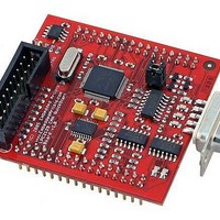
EA-QSB-103
Specifications of EA-QSB-103


Related parts for EA-QSB-103


EA-QSB-103 Summary of contents
Page 1
... Key features brought by LPC2109/2119/2129/01 devices I Fast GPIO ports enable port pin toggling up to 3.5 times faster than the original device. They also allow for a port pin to be read at any time regardless of its function. I Dedicated result registers for ADC(s) reduce interrupt overhead. The ADC pads are 5 V tolerant when confi ...
Page 2
... EmbeddedICE-RT interface enables breakpoints and watch points. Interrupt service routines can continue to execute while the foreground task is debugged with the on-chip RealMonitor software. I Embedded Trace Macrocell (ETM) enables non-intrusive high speed real-time tracing of instruction execution. I Two interconnected CAN interfaces (one for LPC2109) with advanced acceptance fi ...
Page 3
... Package Name Description LQFP64 plastic low profile quad flat package; 64 leads; body 10 LQFP64 plastic low profile quad flat package; 64 leads; body 10 LQFP64 plastic low profile quad flat package; 64 leads; body 10 Ordering options Flash RAM CAN memory channel 8 kB ...
Page 4
... INTERRUPT CONTROLLER Bus (AHB) AHB DECODER 2 I C-BUS SERIAL INTERFACE (4) SPI1/SSP SERIAL INTERFACE SPI0 SERIAL INTERFACE UART0/UART1 WATCHDOG TIMER SYSTEM CONTROL REAL-TIME CLOCK 002aad172 © NXP B.V. 2007. All rights reserved. (1) SCL (1) SDA (1) SCK1 (1) MOSI1 (1) MISO1 (1) SSEL1 (1) SCK0 (1) MOSI0 (1) MISO0 ...
Page 5
NXP Semiconductors 5. Pinning information 5.1 Pinning P0[21]/PWM5/CAP1[3] 1 P0[22]/CAP0[0]/MAT0[0] 2 (1) 3 P0[23]/RD2 P1[19]/TRACEPKT3 4 (1) P0[24]/TD2 DDA(3V3) P1[18]/TRACEPKT2 8 P0[25]/RD1 9 10 TD1 P0[27]/AIN0/CAP0[1]/MAT0[1] 11 P1[17]/TRACEPKT1 12 P0[28]/AIN1/CAP0[2]/MAT0[ P0[29]/AIN2/CAP0[3]/MAT0[3] P0[30]/AIN3/EINT3/CAP0[0] ...
Page 6
... LPC2109_2119_2129_6 Product data sheet Type Description I/O Port 32-bit bidirectional I/O port with individual direction controls for each bit. The operation of port 0 pins depends upon the pin function selected via the Pin Connect Block. Pins 26 and 31 of port 0 are not available. O TXD0 — ...
Page 7
... CAP0[0] — Capture input for Timer 0, channel 0. I/O Port 32-bit bidirectional I/O port with individual direction controls for each bit. The operation of port 1 pins depends upon the pin function selected via the Pin Connect Block. Pins 0 through 15 of port 1 are not available. ...
Page 8
NXP Semiconductors Table 3. Pin description …continued Symbol Pin P1[16]/ 16 TRACEPKT0 P1[17]/ 12 TRACEPKT1 P1[18]/ 8 TRACEPKT2 P1[19]/ 4 TRACEPKT3 P1[20]/ 48 TRACESYNC P1[21]/ 44 PIPESTAT0 P1[22]/ 40 PIPESTAT1 P1[23]/ 36 PIPESTAT2 P1[24]/ 32 TRACECLK P1[25]/EXTIN0 28 P1[26]/RTCK 24 ...
Page 9
NXP Semiconductors Table 3. Pin description …continued Symbol Pin V 63 DDA(1V8) V 23, 43, 51 DD(3V3 DDA(3V3) [1] SSP interface available on LPC2109/01, LPC2119/01, and LPC2129/01 only. LPC2109_2119_2129_6 Product data sheet Type Description I Analog 1.8 V ...
Page 10
... It may be programmed In System via the serial port. The application program may also erase and/or program the flash while the application is running, allowing a great degree of flexibility for data storage field firmware upgrades, etc. When on-chip bootloader is used, 60/120/248 kB of flash memory is available for user code. The LPC2109/2119/2129 fl ...
Page 11
NXP Semiconductors However, the ISP flash erase command can be executed at any time (no matter whether the CRP off). Removal of CRP is achieved by erasure of full on-chip user flash. With the CRP off, full ...
Page 12
... FIQ latency is achieved when only one request is classified as FIQ because then the FIQ service routine can simply start dealing with that device. But if more than one request is assigned to the FIQ class, the FIQ service routine can read a word from the VIC that identifies which FIQ source(s) is (are) requesting an interrupt. ...
Page 13
... Non-vectored IRQs have the lowest priority. The VIC combines the requests from all the vectored and non-vectored IRQs to produce the IRQ signal to the ARM processor. The IRQ service routine can start by reading a register from the VIC and jumping there. If any of the vectored IRQs are requesting, the ...
Page 14
... Device pins that are not connected to a specific peripheral function are controlled by the parallel I/O registers. Pins may be dynamically configured as inputs or outputs. Separate registers allow setting or clearing any number of outputs simultaneously. The value of the output register may be read back, as well as the current state of the port pins. 6.7.1 Features • ...
Page 15
... The LPC2119 and LPC2129 each contain two CAN controllers, while the LPC2109 has one CAN controller. The CAN is a serial communications protocol which efficiently supports distributed real-time control with a very high level of security. Its domain of application ranges from high-speed networks to low-cost multiplex wiring. ...
Page 16
... The I C-bus is a bidirectional bus for inter-IC control using only two wires: a serial clock line (SCL), and a serial data line (SDA). Each device is recognized by a unique address and can operate as either a receiver-only device (e.g. an LCD driver or a transmitter with the capability to both receive and send information (such as memory). Transmitters and/or receivers can operate in either master or slave mode, depending on whether the chip has to initiate a data transfer or is only addressed ...
Page 17
... NXP Semiconductors 6.12 SPI serial I/O controller The LPC2109/2119/2129 each contain two SPIs. The SPI is a full duplex serial interface, designed to be able to handle multiple masters and slaves connected to a given bus. Only a single master and a single slave can communicate on the interface during a given data transfer ...
Page 18
... Features available in LPC2109/2119/2129/01 only The LPC2109/2119/2129/01 can count external events on one of the capture inputs if the external pulse lasts at least one half of the period of the PCLK. In this configuration, unused capture lines can be selected as regular timer capture inputs, or used as external interrupts. ...
Page 19
... Selectable time period from (T T cy(PCLK) 6.16 Real-time clock The RTC is designed to provide a set of counters to measure time when normal or idle operating mode is selected. The RTC has been designed to use little power, making it suitable for battery powered systems where the CPU is not running continuously (Idle mode). ...
Page 20
... Again, the MR0 match register controls the PWM cycle rate. The other match registers control the two PWM edge positions. Additional double edge controlled PWM outputs require only two match registers each, since the repetition rate is the same for all PWM outputs. ...
Page 21
... This is important at power on, all types of Reset, and whenever any of the aforementioned functions are turned off for any reason. Since the oscillator and other functions are turned off during Power-down mode, any wake-up of the processor from Power-down mode makes use of the Wake-up Timer ...
Page 22
... IAP calls or call reinvoke ISP command to enable flash update via UART0. CAUTION If level three Code Read Protection (CRP3) is selected, no future factory testing can be performed on the device. Remark: Devices without the suffix /00 or /01 have only a security level equivalent to CRP2 available ...
Page 23
... The LPC2109/2119/2129 support emulation and debugging via a JTAG serial port. A trace port allows tracing program execution. Debugging and trace functions are multiplexed only with GPIOs on Port 1. This means that all communication, timer and interface peripherals residing on Port 0 are available during the development and debugging phase as they are when the application is run in the embedded system itself ...
Page 24
... RealMonitor RealMonitor is a configurable software module, developed by ARM Inc., which enables real time debug lightweight debug monitor that runs in the background while users debug their foreground application. It communicates with the host using the DCC (Debug Communications Channel), which is present in the EmbeddedICE logic. The LPC2109/2119/2129 contain a specifi ...
Page 25
... This product includes circuitry specifically designed for the protection of its internal devices from the damaging effects of excessive static charge. Nonetheless suggested that conventional precautions be taken to avoid applying greater than the rated maximum. b) Parameters are valid over operating temperature range unless otherwise specified. All voltages are with respect to V otherwise noted ...
Page 26
NXP Semiconductors 8. Static characteristics Table 6. Static characteristics +85 C for industrial applications, unless otherwise specified. amb Symbol Parameter V supply voltage (1.8 V) DD(1V8) V supply voltage (3.3 V) DD(3V3) V analog supply ...
Page 27
... HIGH-level input voltage IH V LOW-level input voltage IL V hysteresis voltage hys V LOW-level output voltage OL I input leakage current LI Oscillator pins V input voltage on pin i(XTAL1) XTAL1 V output voltage on pin o(XTAL2) XTAL2 [1] Typical ratings are not guaranteed. The values listed are at room temperature (25 C), nominal supply voltages. ...
Page 28
... C to +85 C unless otherwise specified. ADC frequency amb Conditions ) is the difference between the actual step width and the ideal step width. See ) is the peak difference between the center of the steps of the actual and the ideal transfer curve after Figure 4. Figure Figure 4. Rev. 06 — ...
Page 29
... E O (1) Example of an actual transfer curve. (2) The ideal transfer curve. (3) Differential linearity error (E (4) Integral non-linearity (E L(adj) (5) Center of a step of the actual transfer curve. Fig 4. ADC characteristics LPC2109_2119_2129_6 Product data sheet (2) (5) (4) (3) 1 LSB (ideal (LSB ) ...
Page 30
... LPC2129/01 devices The power consumption measurements represent typical values for the given conditions. The peripherals were enabled through the PCONP register, but for these measurements, the peripherals were not configured to run. Peripherals were disabled through the PCONP register. Refer to the LPC2119/2129/2194/2292/2294 User Manual for a description of the PCONP register ...
Page 31
... Fig 8. Typical LPC2109/01 I DD(idle) LPC2109_2119_2129_6 Product data sheet all peripherals enabled all peripherals disabled 28 36 measured at different frequencies 60 MHz 48 MHz 12 MHz 1.75 1.80 measured at different voltages Rev. 06 — 10 December 2007 LPC2109/2119/2129 Single-chip 16/32-bit microcontrollers 002aad129 44 52 frequency (MHz) CCLK ; 4 002aad130 1.85 1.90 ...
Page 32
... Fig 10. Typical LPC2119/01 and LPC2129/01 I LPC2109_2119_2129_6 Product data sheet all peripherals enabled all peripherals disabled 28 36 measured at different frequencies DD(act) 60 MHz 48 MHz 12 MHz 1.75 1.80 measured at different voltages DD(act) Rev. 06 — 10 December 2007 LPC2109/2119/2129 Single-chip 16/32-bit microcontrollers 002aad131 44 52 frequency (MHz) CCLK ; 4 002aad132 1.85 1 ...
Page 33
... Fig 12. Typical LPC2119/01 and LPC2129/01 I LPC2109_2119_2129_6 Product data sheet all peripherals enabled all peripherals disabled 28 36 measured at different frequencies DD(idle) 60 MHz 48 MHz 12 MHz 1.75 1.80 measured at different voltages DD(idle) Rev. 06 — 10 December 2007 LPC2109/2119/2129 Single-chip 16/32-bit microcontrollers 002aad133 44 52 frequency (MHz) CCLK ; 4 002aad134 1.85 1 ...
Page 34
... Fig 14. Typical LPC2109/01, LPC2119/01, and LPC2129/01 I LPC2109_2119_2129_6 Product data sheet 60 MHz 48 MHz 12 MHz 1.75 1.80 measured at different voltages DD(act) 60 MHz 48 MHz 12 MHz 1.75 1.80 measured at different voltages DD(idle) Rev. 06 — 10 December 2007 LPC2109/2119/2129 Single-chip 16/32-bit microcontrollers 002aad135 1.85 1.90 voltage (V) CCLK ; 4 002aad136 1.85 1.90 ...
Page 35
... Product data sheet LPC2109/2119/2129 Single-chip 16/32-bit microcontrollers 60 MHz 48 MHz 12 MHz 10 35 CCLK measured at different temperatures DD(act) 60 MHz 48 MHz 12 MHz 10 35 CCLK measured at different temperatures DD(idle) Rev. 06 — 10 December 2007 002aad137 60 85 temperature ( 002aad138 60 85 temperature ( © NXP B.V. 2007. All rights reserved ...
Page 36
... Core voltage 1 Peripheral Timer0 Timer1 UART0 UART1 PWM0 2 I C-bus SPI0/1 LPC2109_2119_2129_6 Product data sheet 10 Typical LPC2109/01 peripheral power consumption in active mode = 25 C; all measurements in A; PCLK = amb CCLK = 12 MHz 103 103 230 Typical LPC2119/01 and LPC2129/01 peripheral power consumption in active mode = 25 C ...
Page 37
... NXP Semiconductors Table 9. Core voltage 1 Peripheral RTC ADC CAN1/2 LPC2109_2119_2129_6 Product data sheet Typical LPC2119/01 and LPC2129/01 peripheral power consumption in active mode …continued = 25 C; all measurements in A; PCLK = amb CCLK = 12 MHz 16 33 229 Rev. 06 — 10 December 2007 LPC2109/2119/2129 Single-chip 16/32-bit microcontrollers CCLK . 4 ...
Page 38
NXP Semiconductors 9. Dynamic characteristics Table 10. Dynamic characteristics +85 C for industrial applications; V amb Symbol Parameter External clock f oscillator frequency osc T clock cycle time cy(clk) t clock HIGH time CHCX t ...
Page 39
NXP Semiconductors 9.1 Timing V Fig 18. External clock timing LPC2109_2119_2129_6 Product data sheet 0 0.2V 0 0. CHCL Rev. 06 — 10 December 2007 LPC2109/2119/2129 Single-chip 16/32-bit microcontrollers t ...
Page 40
... NXP Semiconductors 10. Package outline LQFP64: plastic low profile quad flat package; 64 leads; body 1 pin 1 index DIMENSIONS (mm are the original dimensions) A UNIT max. 0.20 1.45 mm 1.6 0.25 0.05 1.35 Note 1. Plastic or metal protrusions of 0.25 mm maximum per side are not included. OUTLINE VERSION ...
Page 41
... TTL UART LPC2109_2119_2129_6 Product data sheet Abbreviations Description Analog-to-Digital Converter Advanced Microcontroller Bus Architecture Advanced Peripheral Bus Controller Area Network Central Processing Unit Debug Communications Channel First In, First Out General Purpose Input/Output Input/Output Phase-Locked Loop Pulse Width Modulator Random Access Memory ...
Page 42
... Type number LPC2119FBD64/01 has been added. • Type number LPC2129FBD64/01 has been added. • Details introduced with /01 devices on new peripherals/features (Fast I/O Ports, SSP, CRP) and enhancements to existing ones (UART0/1, Timers, ADC, and SPI) have been added. • Power measurements for LPC2109/2119/2129/01 devices have been added. ...
Page 43
... Qualification Product [short] data sheet Production [1] Please consult the most recently issued document before initiating or completing a design. [2] The term ‘short data sheet’ is explained in section “Definitions”. [3] The product status of device(s) described in this document may have changed since this document was published and may differ in case of multiple devices. The latest product status information is available on the Internet at URL http://www.nxp.com. 13.2 Defi ...
Page 44
... NXP Semiconductors 15. Contents 1 General description . . . . . . . . . . . . . . . . . . . . . . 1 2 Features . . . . . . . . . . . . . . . . . . . . . . . . . . . . . . . 1 2.1 Key features brought by LPC2109/2119/2129/01 devices . . . . . . . . . . . . . . . . . . . . . . . . . . . . . . . 1 2.2 Key features common for all devices . . . . . . . . 1 3 Ordering information . . . . . . . . . . . . . . . . . . . . . 2 3.1 Ordering options . . . . . . . . . . . . . . . . . . . . . . . . 3 4 Block diagram . . . . . . . . . . . . . . . . . . . . . . . . . . 4 5 Pinning information . . . . . . . . . . . . . . . . . . . . . . 5 5.1 Pinning . . . . . . . . . . . . . . . . . . . . . . . . . . . . . . . 5 5.2 Pin description . . . . . . . . . . . . . . . . . . . . . . . . . 6 6 Functional description . . . . . . . . . . . . . . . . . . 10 6.1 Architectural overview ...