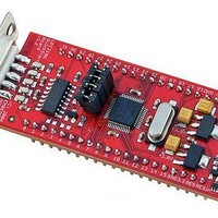
EA-QSB-102 Embedded Artists, EA-QSB-102 Datasheet
EA-QSB-102
Specifications of EA-QSB-102


Related parts for EA-QSB-102


EA-QSB-102 Summary of contents
Page 1
... New features implemented in LPC2104/2105/2106/01 devices I Fast GPIO port enables port pin toggling up to 3.5 times faster than the original device and also allows for a port pin to be read at any time regardless of its function. I UART 0/1 include fractional baud rate generator, autobauding capabilities, and handshake fl ...
Page 2
... Embedded Trace Macrocell enables non-intrusive high speed real-time tracing of instruction execution. I Multiple serial interfaces including two UARTs (16C550), Fast I SPI. I Two 32-bit timers (7 capture/compare channels), PWM unit (6 outputs), Real Time Clock and Watchdog thirty-two 5 V tolerant general purpose I/O pins in a tiny LQFP48 (7 mm package MHz maximum CPU clock available from programmable on-chip Phase-Locked Loop with settling time of 100 s ...
Page 3
... LPC2104_2105_2106_7 Product data sheet Ordering information …continued Package Name Description LQFP48 plastic low profile quad flat package; 48 leads; body 7 7 LQFP48 plastic low profile quad flat package; 48 leads; body 7 7 HVQFN48 plastic thermal enhanced very thin quad flat package; no leads; 48 terminals; body ...
Page 4
... MAT0[2:0] TIMER 0/TIMER 1 (1) MAT1[3:0] GENERAL P0[31:0] PURPOSE I/O (1) PWM0 PWM[6:1] REAL-TIME CLOCK (1) Shared with GPIO. (2) When test/debug interface is used, GPIO/other functions sharing these pins are not available. (3) Available on LPC2104/2105/2106/01 only. Fig 1. Block diagram LPC2104_2105_2106_7 Product data sheet (2) (2) TMS TDI ...
Page 5
NXP Semiconductors 5. Pinning information 5.1 Pinning P0.19/MAT1.2/TCK P0.20/MAT1.3/TDI P0.21/PWM5/TDO V P0.27/TRACEPKT0/TRST P0.28/TRACEPKT1/TMS P0.29/TRACEPKT2/TCK Pin configuration is identical for all LQFP48 packages. Fig 2. Pin configuration (LQFP48) LPC2104_2105_2106_7 Product data sheet n. DD(1V8) RESET 6 ...
Page 6
... NXP Semiconductors terminal 1 index area P0.19/MAT1.2/TCK P0.20/MAT1.3/TDI P0.21/PWM5/TDO P0.27/TRACEPKT0/TRST P0.28/TRACEPKT1/TMS P0.29/TRACEPKT2/TCK Pin configuration is identical for LPC2106FHN48, LPC2106FHN48/00, and LPC2106FHN48/01. Fig 3. Pin configuration (HVQFN48) LPC2104_2105_2106_7 Product data sheet n. DD(1V8) RESET 6 LPC2104/2105/2106 XTAL1 11 12 XTAL2 Transparent top view Rev. 07 — 20 June 2008 ...
Page 7
... Product data sheet Type Description I/O Port 0: Port 32-bit bidirectional I/O port with individual direction controls for each bit. The operation of port 0 pins depends upon the pin function selected via the Pin Connect Block. I/O P0.0 — Port 0 bit 0. O TXD0 — Transmitter output for UART 0. ...
Page 8
... DSR1 — Data Set Ready input for UART 1. O MAT1.0 — Match output for Timer 1, channel 0. I/O P0.13 — Port 0 bit 13. O DTR1 — Data Terminal Ready output for UART 1. O MAT1.1 — Match output for Timer 1, channel 1. I/O P0.14 — Port 0 bit 14. I DCD1 — ...
Page 9
NXP Semiconductors Table 3. Pin description …continued Symbol Pin [4] P0.26/TRACESYNC 39 [4] P0.27/TRACEPKT0/ 8 TRST [4] P0.28/TRACEPKT1/ 9 TMS [4] P0.29/TRACEPKT2/ 10 TCK [4] P0.30/TRACEPKT3/ 15 TDI [4] P0.31/EXTIN0/TDO 16 [4] RTCK 26 DBGSEL 27 [5] RESET 6 XTAL1 ...
Page 10
... It may be programmed In System via the serial port. The application program may also erase and/or program the flash while the application is running, allowing a great degree of flexibility for data storage field firmware upgrades, etc. When on-chip bootloader is used, 120 kB of flash memory is available for user code. ...
Page 11
NXP Semiconductors 6.4 Memory map The LPC2104/2105/2106 memory maps incorporate several distinct regions, as shown in the following figures. In addition, the CPU interrupt vectors may be re-mapped to allow them to reside in either flash memory (the default) or ...
Page 12
... FIQ service routine can simply start dealing with that device. But if more than one request is assigned to the FIQ class, the FIQ service routine can read a word from the VIC that identifies which FIQ source(s) is (are) requesting an interrupt. ...
Page 13
... Name Description PINSEL0 Pin function select register 0 PINSEL1 Pin function select register 1 Table 6 Rev. 07 — 20 June 2008 LPC2104/2105/2106 Single-chip 32-bit microcontrollers [1] [1] [1] Table 5. are reserved, and should not be used VIC channel # Access Read/Write Read/Write © NXP B.V. 2008. All rights reserved ...
Page 14
NXP Semiconductors Table 6. PINSEL0 1:0 3:2 5:4 7:6 9:8 11:10 13:12 15:14 17:16 19:18 21:20 23:22 25:24 LPC2104_2105_2106_7 Product data sheet Pin function select register 0 (PINSEL0 - 0xE002 C000) Pin name Value P0 ...
Page 15
NXP Semiconductors Table 6. PINSEL0 27:26 29:28 31:30 6.8 Pin function select register 1 (PINSEL1 - 0xE002 C004) The PINSEL1 register controls the functions of the pins as per the settings listed in Table 7. The direction control bit in ...
Page 16
... Device pins that are not connected to a specific peripheral function are controlled by the GPIO registers. Pins may be dynamically configured as inputs or outputs. Separate registers allow setting or clearing any number of outputs simultaneously. The value of the output register may be read back, as well as the current state of the port pins. 6.9.1 Features • ...
Page 17
... bidirectional bus for inter-IC control using only two wires: a serial clock line (SCL), and a serial data line (SDA). Each device is recognized by a unique address and can operate as either a receiver-only device (e.g. an LCD driver or a transmitter with the capability to both receive and send information (such as memory). Transmitters and/or receivers can operate in either master or slave mode, depending on whether the chip has to initiate a data transfer or is only addressed ...
Page 18
... Combined SPI master and slave. • Maximum data bit rate of one eighth of the input clock rate. 6.12.2 Features available in LPC2104/2105/2106/01 only • Selectable transfer width of eight to 16 bit per frame. • When the SPI interface is used in Master mode, the SSEL pin is not needed (can be used for a different function) ...
Page 19
... Features available in LPC2104/2105/2106/01 only The LPC2104/2105/2106/01 can count external events on one of the capture inputs if the external pulse lasts at least one half of the period of the PCLK. In this configuration, unused capture lines can be selected as regular timer capture inputs or used as external interrupts. ...
Page 20
... Again, the MR0 match register controls the PWM cycle rate. The other match registers control the two PWM edge positions. Additional double edge controlled PWM outputs require only two match registers each, since the repetition rate is the same for all PWM outputs. ...
Page 21
... Supports single edge controlled and/or double edge controlled PWM outputs. Single edge controlled PWM outputs all go HIGH at the beginning of each cycle unless the output is a constant LOW. Double edge controlled PWM outputs can have either edge occur at any position within a cycle. This allows for both positive going and negative going pulses. • ...
Page 22
... This is important at power on, all types of Reset, and whenever any of the aforementioned functions are turned off for any reason. Since the oscillator and other functions are turned off during Power-down mode, any wake-up of the processor from Power-down mode makes use of the wake-up timer ...
Page 23
... IAP calls or a call to reinvoke ISP command to enable flash update via UART 0. CAUTION If level three Code Read Protection (CRP3) is selected, no future factory testing can be performed on the device. 6.18.5 External interrupt inputs The LPC2104/2105/2106 include three external interrupt inputs as selectable pin functions ...
Page 24
... Emulation and debugging The LPC2104/2105/2106 support emulation and debugging via a JTAG serial port. A trace port allows tracing program execution. Each of these functions requires a trade-off of debugging features versus device pins. Because the LPC2104/2105/2106 are provided in a small package, there is no room for permanently assigned JTAG or Trace pins. An ...
Page 25
... RealMonitor RealMonitor is a configurable software module, developed by ARM Inc., which enables real time debug lightweight debug monitor that runs in the background while users debug their foreground application. It communicates with the host using the DCC (Debug Communications Channel), which is present in the EmbeddedICE logic. The LPC2104/2105/2106 contain a specifi ...
Page 26
... This product includes circuitry specifically designed for the protection of its internal devices from the damaging effects of excessive static charge. Nonetheless suggested that conventional precautions be taken to avoid applying greater than the rated maximum. b) Parameters are valid over operating temperature range unless otherwise specified. All voltages are with respect to V otherwise noted ...
Page 27
NXP Semiconductors 8. Static characteristics Table 9. Static characteristics +70 C for commercial applications, unless otherwise specified. amb Symbol Parameter V supply voltage (1.8 V) DD(1V8) V supply voltage (3.3 V) DD(3V3) Standard port pins, ...
Page 28
... I C-bus pins V HIGH-state input voltage IH V LOW-state input voltage IL V hysteresis voltage hys V LOW-state output voltage OL I input leakage current LI LPC2104_2105_2106_7 Product data sheet …continued Conditions = 1.8 V; DD(1V8) CCLK = 60 MHz code amb while(1){} executed from flash; all peripherals enabled via PCONP register but not confi ...
Page 29
... The power consumption measurements represent typical values for the given conditions. The peripherals were enabled through the PCONP register, but for these measurements the peripherals were not configured to run. Power measurements with all peripherals enabled were performed with the SPI enabled and the SSP disabled. Peripherals were disabled through the PCONP register ...
Page 30
... Test conditions: Idle mode entered executing code from on-chip flash; PCLK = core voltage 1.8 V. amb Typical LPC2104/2105/2106/01 I Rev. 07 — 20 June 2008 LPC2104/2105/2106 Single-chip 32-bit microcontrollers 60 MHz 48 MHz 12 MHz 1.80 1.85 1.90 core voltage (V) measured at different core voltages DD(act) 44 frequency (MHz) measured at different frequencies DD(idle) 002aad710 1.95 CCLK ; 4 002aad711 60 CCLK ; ...
Page 31
... Test conditions: Active mode entered executing code from on-chip flash; PCLK = voltage 1.8 V; all peripherals disabled. Typical LPC2104/2105/2106/01 I Rev. 07 — 20 June 2008 LPC2104/2105/2106 Single-chip 32-bit microcontrollers 60 MHz 48 MHz 12 MHz 1.80 1.85 1.90 core voltage (V) measured at different core voltages DD(idle temperature ( C) measured at different temperatures DD(act) 002aad712 1.95 CCLK ; 4 002aad713 ...
Page 32
... Test conditions: Power-down mode entered executing code from on-chip flash. different temperatures Typical LPC2104/2105/2106/01 peripheral power consumption in Idle mode = 25 C; all measurements in mA; PCLK = amb Rev. 07 — 20 June 2008 LPC2104/2105/2106 Single-chip 32-bit microcontrollers 35 60 temperature ( C) measured at different temperatures DD(idle) 1 ...
Page 33
NXP Semiconductors Table 10. Peripheral PWM0 2 I C-bus SPI RTC SSP LPC2104_2105_2106_7 Product data sheet Typical LPC2104/2105/2106/01 peripheral power consumption in Idle mode …continued Rev. 07 — 20 June 2008 LPC2104/2105/2106 Single-chip 32-bit microcontrollers CCLK = 60 MHz 0.511 ...
Page 34
NXP Semiconductors 9. Dynamic characteristics Table 11. Dynamic characteristics +70 C for commercial applications +85 C for industrial applications; V amb [1] specified ranges. Symbol Parameter External clock f oscillator frequency osc ...
Page 35
... NXP Semiconductors 9.1 Timing Fig 12. External clock timing (with an amplitude of at least V LPC2104_2105_2106_7 Product data sheet LPC2104/2105/2106 t CHCX CHCL CLCX CLCH T cy(clk) = 200 mV) i(RMS) Rev. 07 — 20 June 2008 Single-chip 32-bit microcontrollers 002aaa907 © NXP B.V. 2008. All rights reserved ...
Page 36
... NXP Semiconductors 10. Package outline LQFP48: plastic low profile quad flat package; 48 leads; body 1 pin 1 index DIMENSIONS (mm are the original dimensions) A UNIT max. 0.20 1.45 1.6 mm 0.25 0.05 1.35 Note 1. Plastic or metal protrusions of 0.25 mm maximum per side are not included. OUTLINE VERSION ...
Page 37
... NXP Semiconductors HVQFN48: plastic thermal enhanced very thin quad flat package; no leads; 48 terminals; body 0.85 mm terminal 1 index area terminal 1 48 index area DIMENSIONS (mm are the original dimensions) (1) A UNIT max. 0.05 0. 0.2 0.00 0.18 Note 1. Plastic or metal protrusions of 0.075 mm maximum per side are not included. ...
Page 38
NXP Semiconductors 11. Abbreviations Table 12. Acronym AMBA APB CPU DCC FIFO GPIO PLL PWM RAM SPI SSI SSP SRAM TTL UART LPC2104_2105_2106_7 Product data sheet Abbreviations Description Advanced Microcontroller Bus Architecture ARM Peripheral Bus Central Processing Unit Debug Communications ...
Page 39
... Parts LPC2104FBD48/01, LPC2105FBD48/01, LPC2106BBD48, LPC2106FBD48/01, and LPC2106FHN48/01 added. Description of /01 features added. LPC2104/2105/2106/01 power consumption measurements added. Maximum frequency f for external oscillator and external crystal updated. osc Figure 12 “External clock timing (with an amplitude of at least V updated. Condition for I and I updated in OHS OLS ...
Page 40
... Qualification Product [short] data sheet Production [1] Please consult the most recently issued document before initiating or completing a design. [2] The term ‘short data sheet’ is explained in section “Definitions”. [3] The product status of device(s) described in this document may have changed since this document was published and may differ in case of multiple devices. The latest product status information is available on the Internet at URL http://www.nxp.com. 13.2 Defi ...
Page 41
... NXP Semiconductors 15. Contents 1 General description . . . . . . . . . . . . . . . . . . . . . . 1 2 Features . . . . . . . . . . . . . . . . . . . . . . . . . . . . . . . 1 2.1 New features implemented in LPC2104/2105/2106/01 devices 2.2 Key common features . . . . . . . . . . . . . . . . . . . . 1 3 Ordering information . . . . . . . . . . . . . . . . . . . . . 2 3.1 Ordering options . . . . . . . . . . . . . . . . . . . . . . . . 3 4 Block diagram . . . . . . . . . . . . . . . . . . . . . . . . . . 4 5 Pinning information . . . . . . . . . . . . . . . . . . . . . . 5 5.1 Pinning . . . . . . . . . . . . . . . . . . . . . . . . . . . . . . . 5 5.2 Pin description . . . . . . . . . . . . . . . . . . . . . . . . . 7 6 Functional description . . . . . . . . . . . . . . . . . . 10 6.1 Architectural overview 6.2 On-chip fl ...