MF1PLUS8031DA4/03, NXP Semiconductors, MF1PLUS8031DA4/03, Datasheet
MF1PLUS8031DA4/03,
Specifications of MF1PLUS8031DA4/03,


Related parts for MF1PLUS8031DA4/03,


MF1PLUS8031DA4/03, Summary of contents
Page 1
MF1PLUSx0y1 Mainstream contactless smart card IC for fast and easy solution development Rev. 3.1 — 19 April 2010 163531 1. General description Migrate classic contactless smart card systems to the next security level! MIFARE Plus brings benchmark security to mainstream ...
Page 2
... NXP Semiconductors Number of single write operations: 200000 cycles (typical) Common Criteria Certification: EAL4+ 3. Applications Public transportation Access management such as employee, school or campus cards Electronic toll collection Closed loop micro payment Car parking Internet cafés Loyalty programs 4. Quick reference data Table 1. ...
Page 3
... NXP Semiconductors 5. Ordering information Table 2. Ordering information Type number Package Commercial name MF1PLUS8001DUD/03 FFC MF1PLUS8001DA4/03 MOA4 MF1PLUS8011DUD/03 FFC MF1PLUS8021DUD/03 FFC MF1PLUS8011DA4/03 MOA4 MF1PLUS8021DA4/03 MOA4 MF1PLUS6001DUD/03 FFC MF1PLUS6001DA4/03 MOA4 MF1PLUS6011DUD/03 FFC MF1PLUS6021DUD/03 FFC MF1PLUS6011DA4/03 MOA4 MF1PLUS6021DA4/03 MOA4 MF1PLUSX0Y1_SDS_31 Product short data sheet ...
Page 4
... NXP Semiconductors Table 2. Ordering information Type number Package Commercial name MF1PLUS8001DUD/13 FFC MF1PLUS8001DA4/13 MOA4 MF1PLUS6001DUD/13 FFC MF1PLUS6001DA4/13 MOA4 6. Block diagram INTERFACE SECURITY SENSORS POWER ON REGULATOR INPUT FILTER GENERATOR Fig 1. MF1PLUSX0Y1_SDS_31 Product short data sheet PUBLIC …continued Name Description - 8 inch wafer (sawn; 120 µm thickness, on film frame carrier ...
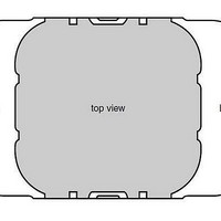
Page 5
... NXP Semiconductors 7. Pinning information 7.1 Smart card contactless module Fig 2. Table 3. Contactless interface module Antenna contacts LA LB MF1PLUSX0Y1_SDS_31 Product short data sheet PUBLIC LA Contact assignments for SOT500-2 (MOA4) Bonding pad assignments to smart card contactless module MF1PLUSx0y1DA4/03 and /13 Symbol Description LA antenna coil connection LA ...
Page 6
... NXP Semiconductors 8. Functional description 8.1 Memory organization The 4 kB EEPROM memory (MF1PLUS80x) is organized in 32 sectors of 4 blocks and in 8 sectors of 16 blocks. The 2 kB EEPROM memory (MF1PLUS60x) is organized in 32 sectors of 4 blocks. One block consists of 16 bytes. SECTOR BLOCK ... ... ...
Page 7
... NXP Semiconductors Value blocks are special counters where the stored value can be manipulated with specific commands such as MF Increment, MF Decrement and MF Transfer. These value blocks have a fixed data format enabling error detection and correction with backup management to be performed. The MIFARE Plus X provides two further commands which can be used to optimize performance when using value blocks. These are: • ...
Page 8
... NXP Semiconductors 8.1.6 Originality function The originality function is implemented by an AES authentication with the originality key. The authentication is performed in ISO/IEC 14443-4 protocol layer. 8.2 Card activation and communication protocol The ISO/IEC 14443-3 anticollision mechanism allows for simultaneous handling of multiple PICCs in the field. The anticollision algorithm selects each PICC individually and ensures that execution of a transaction with a selected PICC is performed correctly without data corruption from other PICCs in the field ...
Page 9
... NXP Semiconductors 8.2.2 ISO/IEC 14443-4 Protocol The ISO/IEC 14443-4 Protocol (also known as T=CL) is used in many processor cards. This protocol is used for the MIFARE Plus with the following security levels: • Security Level 0: all commands • Security Level 1: only the security level switch and originality function • ...
Page 10
... The access conditions are set in the sector trailer as in MIFARE Classic 1K and MIFARE Classic 4K. Using the originality function possible to verify that the chip is a genuine NXP Semiconductors MIFARE Plus. 8.7 Security level 3 The operation in security level 3 is solely based on the ISO/IEC 14443-4 protocol layer. ...
Page 11
... NXP Semiconductors These two session keys are used to secure the data which is exchanged on the interface between the card and reader. One of the two keys is used to ensure the confidentiality of the command and the response while the other key ensures the integrity of the command and the response ...
Page 12
... NXP Semiconductors 9.2 Security level ISO/IEC 14443-4 Table 5. Command RATS PPS DESELECT Please find more information on ISO/IEC 14443-3 in ATQA, SAK and ATS in 9.3 Security level 0 command overview Table 6. Command Write Perso Commit Perso First Authenticate (part 1) Following Authenticate (part 1) following authenticate Authenticate (part 2) 9 ...
Page 13
... NXP Semiconductors 9.5 Security level 2 command overview Table 8. Command Commands using backwards compatibility protocol; see Following Authenticate (part 1) following authenticate Authenticate (part 2) MF1ICS50xx, MF1ICS70xx commands MF Authenticate Key A MF Authenticate Key B MF Read MF Write MF Decrement MF Increment MF Restore MF Transfer Multi Block Read Multi Block Write ...
Page 14
... NXP Semiconductors Table 9. Command Read Plain UnMACed, Response MACed Write commands Write Write MACed Write Plain Write Plain MACed VALUE operations Increment Increment MACed Decrement Decrement MACed Transfer Transfer MACed Increment Transfer Increment Transfer MACed Decrement Transfer Decrement Transfer MACed Restore ...
Page 15
... NXP Semiconductors 10. Limiting values Table 10. In accordance with the Absolute Maximum Rating System (IEC 60134). Symbol /pack tot T stg T amb V ESD I lu [1] Stresses above one or more of the limiting values may cause permanent damage to the device. [2] Exposure to limiting values for extended periods may affect device reliability. ...
Page 16
... NXP Semiconductors 12. References [1] Data sheet — MF1ICS50 Functional specification, BU-ID Doc. No. 0010** [2] Data sheet — MF1ICS70 Functional specification, BU-ID Doc. No. 0435**. [3] Data sheet — M1PLUSx0y1 MIFARE Plus functional specification, BU-ID Doc. No. 1637**. [4] Application note — MIFARE Type identification procedure, BU-ID Doc. No. 1843**. ...
Page 17
... NXP Semiconductors and its customer, unless NXP Semiconductors and customer have explicitly agreed otherwise in writing event however, shall an agreement be valid in which the NXP Semiconductors product is deemed to offer functions and qualities beyond those described in the Product data sheet. ...
Page 18
... NXP Semiconductors’ specifications such use shall be solely at customer’s own risk, and (c) customer fully indemnifies NXP Semiconductors for any liability, damages or failed product claims resulting from customer design and use of the product for automotive applications beyond NXP Semiconductors’ ...
Page 19
... NXP Semiconductors 16. Tables Table 1. Quick reference data . . . . . . . . . . . . . . . . . . . . .2 Table 2. Ordering information . . . . . . . . . . . . . . . . . . . . .3 Table 3. Bonding pad assignments to smart card contactless module . . . . . . . . . . . . . . . . . . . . . . .5 Table 4. ISO/IEC 14443 Table 5. ISO/IEC 14443 .12 Table 6. Security level 0 command overview . . . . . . . . .12 17. Figures Fig 1. Block diagram . . . . . . . . . . . . . . . . . . . . . . . . . . . .4 Fig 2. Contact assignments for SOT500-2 (MOA4 Fig 3. ...
Page 20
... NXP Semiconductors 18. Contents 1 General description . . . . . . . . . . . . . . . . . . . . . . 1 2 Features and benefits . . . . . . . . . . . . . . . . . . . . 1 3 Applications . . . . . . . . . . . . . . . . . . . . . . . . . . . . 2 4 Quick reference data . . . . . . . . . . . . . . . . . . . . . 2 5 Ordering information . . . . . . . . . . . . . . . . . . . . . 3 6 Block diagram . . . . . . . . . . . . . . . . . . . . . . . . . . 4 7 Pinning information . . . . . . . . . . . . . . . . . . . . . . 5 7.1 Smart card contactless module . . . . . . . . . . . . 5 8 Functional description . . . . . . . . . . . . . . . . . . . 6 8.1 Memory organization . . . . . . . . . . . . . . . . . . . . 6 8.1.1 Manufacturer block . . . . . . . . . . . . . . . . . . . . . . 6 8.1.2 Data blocks . . . . . . . . . . . . . . . . . . . . . . . . . . . . 6 8 ...