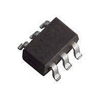
PUMD2 /T2 NXP Semiconductors, PUMD2 /T2 Datasheet - Page 11

PUMD2 /T2
Manufacturer Part Number
PUMD2 /T2
Description
Digital Transistors TRANS RET DOUBLE TAPE-11 REV
Manufacturer
NXP Semiconductors
Datasheet
1.PUMD2165.pdf
(16 pages)
Specifications of PUMD2 /T2
Configuration
Dual
Transistor Polarity
NPN/PNP
Typical Input Resistor
22 KOhms
Typical Resistor Ratio
1
Mounting Style
SMD/SMT
Package / Case
SOT-363-6
Collector- Emitter Voltage Vceo Max
50 V
Peak Dc Collector Current
100 mA
Maximum Operating Temperature
+ 150 C
Minimum Operating Temperature
- 65 C
Lead Free Status / RoHS Status
Lead free / RoHS Compliant
Other names
PUMD2,165
NXP Semiconductors
9. Packing information
10. Soldering
PEMD2_PIMD2_PUMD2_7
Product data sheet
Table 9.
The indicated -xxx are the last three digits of the 12NC ordering code.
[1]
[2]
[3]
Type number Package Description
PEMD2
PIMD2
PUMD2
Fig 14. Reflow soldering footprint PEMD2 (SOT666)
2
For further information and the availability of packing methods, see
T1: normal taping
T2: reverse taping
1.7
1.075
Reflow soldering is the only recommended soldering method.
Packing methods
0.538
SOT666
SOT457
SOT363
0.55
(2 )
Rev. 07 — 24 September 2008
NPN/PNP resistor-equipped transistors; R1 = 22 k , R2 = 22 k
2 mm pitch, 8 mm tape and reel
4 mm pitch, 8 mm tape and reel
4 mm pitch, 8 mm tape and reel; T1
4 mm pitch, 8 mm tape and reel; T2
4 mm pitch, 8 mm tape and reel; T1
4 mm pitch, 8 mm tape and reel; T2
0.45
(4 )
(4 )
0.5
2.75
2.45
2.1
1.6
1.7
PEMD2; PIMD2; PUMD2
0.65
(2 )
(2 )
0.6
(6 )
0.4
0.325
0.25
(2 )
(4 )
Section
0.375
(2 )
(4 )
[2]
[3]
[2]
[3]
0.3
[1]
Packing quantity
3000 4000 8000 10000
-
-
-115
-125
-115
-125
13.
Dimensions in mm
-
-115
-
-
-
-
© NXP B.V. 2008. All rights reserved.
-315
-
-
-
-
-
solder lands
placement area
solder paste
occupied area
sot666_fr
-
-
-135
-165
-135
-165
11 of 16


