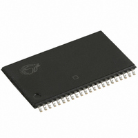
CY7C1049DV33-10ZSXIT Cypress Semiconductor Corp, CY7C1049DV33-10ZSXIT Datasheet - Page 13

CY7C1049DV33-10ZSXIT
Manufacturer Part Number
CY7C1049DV33-10ZSXIT
Description
CY7C1049DV33-10ZSXIT
Manufacturer
Cypress Semiconductor Corp
Specifications of CY7C1049DV33-10ZSXIT
Format - Memory
RAM
Memory Type
SRAM - Asynchronous
Memory Size
4M (512K x 8)
Speed
10ns
Interface
Parallel
Voltage - Supply
3 V ~ 3.6 V
Operating Temperature
-40°C ~ 85°C
Package / Case
44-TSOP II
Memory Configuration
512K X 8
Access Time
10ns
Supply Voltage Range
3V To 3.6V
Memory Case Style
TSOP
No. Of Pins
44
Operating Temperature Range
-40°C To +85°C
Lead Free Status / RoHS Status
Lead free / RoHS Compliant
Available stocks
Company
Part Number
Manufacturer
Quantity
Price
Part Number:
CY7C1049DV33-10ZSXIT
Manufacturer:
CYPRESS/赛普拉斯
Quantity:
20 000
Document History Page
Document Number: 38-05475 Rev. *G
Document Title: CY7C1049DV33, 4-Mbit (512 K × 8) Static RAM
Document Number: 38-05475
REV.
*A
*B
*C
*D
*E
*G
*F
**
ECN NO. Issue Date
1274726
2899972
3059162
3266084
201560
233729
351096
446328
03/29/2010
10/14/2010
05/28/2011
See ECN
See ECN
See ECN
See ECN
See ECN VKN/AESA Corrected typo in the 44-Pin TSOP II pinout
Change
Orig. of
PRAS
PRAS
NXR
SYT
SWI
AJU
PCI
Advance Datasheet for C9 IPP
1.AC, DC parameters are modified as per EROS (Specification # 01-2165)
2.Pb-free offering in the Ordering Information Table
Changed from Advance to Preliminary
Removed 20 ns Speed bin
Corrected DC voltage (min) value in maximum ratings section from - 0.5 to - 0.3V
Redefined I
I
12ns speed bins respectively
I
bins respectively
Added V
Changed reference voltage level for measurement of High Z parameters from 500
mV to 200 mV
Added Data Retention Characteristics, Waveform, and footnotes 11 and 12
Changed Package Diagram name from 44-pin TSOP II Z44 to 44-pin TSOP II ZS44
Changed part names from Z to ZS in the Ordering Information Table
Added 8 ns parts in the Ordering Information Table
Added Pb-free Ordering Information
Shaded Ordering Information Table
Converted from Preliminary to Final
Removed -8 speed bin
Removed Commercial Operating Range product information
Added Automotive Operating Range product information
Updated Thermal Resistance table
Updated footnote #8 on High Z parameter measurement
Replaced Package Name column with Package Diagram in the Ordering Infor-
mation table
Updated
Added
Updated
Updated
AN1064, SRAM System Guidelines for best practice recommendations.”).
Added
Updated in new template.
CC
CC
(Com’l): Changed from 100, 80, and 67 mA to 90, 80 and, 75 mA for 8, 10, and
(Ind’l): Changed from 80 and 67 mA to 90 and 85 mA for 10 and 12ns speed
Ordering Code
Acronyms
IH(max
Package
Package
Functional Description
CC
) specification in Note# 2
values for Com’l and Ind’l temperature ranges
and
Diagrams.
Diagrams.
Units of
Definitions.
Description of Change
Measure.
(Removed “Refer to the Cypress application note
CY7C1049DV33
Page 13 of 14
[+] Feedback


