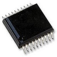
TDA8542TS/N1 NXP Semiconductors, TDA8542TS/N1 Datasheet - Page 7

TDA8542TS/N1
Manufacturer Part Number
TDA8542TS/N1
Description
AMP, AUDIO, PWR, 1.2W, AB, 20SSOP
Manufacturer
NXP Semiconductors
Datasheet
1.TDA8542TSN1.pdf
(20 pages)
Specifications of TDA8542TS/N1
Amplifier Class
AB
No. Of Channels
2
Output Power
1.2W
Load Impedance
16ohm
Operating Temperature Range
-40°C To +85°C
Amplifier Case Style
SSOP
No. Of Pins
20
Base Number
8542
Supply Voltage Range
2.2V To 18V
Thd + N
0.15% @ 0.4W, 8ohm, VCC=5V
Rohs Compliant
Yes
Lead Free Status / RoHS Status
Lead free / RoHS Compliant
Available stocks
Company
Part Number
Manufacturer
Quantity
Price
Company:
Part Number:
TDA8542TS/N1
Manufacturer:
PION
Quantity:
4 015
Philips Semiconductors
AC CHARACTERISTICS
V
Notes
1. Gain of the amplifier is
2. The noise output voltage is measured at the output in a frequency range from 20 Hz to 20 kHz (unweighted), with a
3. Supply voltage ripple rejection is measured at the output, with a source impedance of R
4. Supply voltage ripple rejection is measured at the output, with a source impedance of R
5. Output voltage in mute position is measured with a 1 V (RMS) input voltage in a bandwidth of 20 kHz, so including
1998 Mar 25
P
THD
G
Z
V
SVRR
V
CC
SYMBOL
i(dif)
o
n(o)
o(mute)
cs
2
v(cl)
source impedance of R
The ripple voltage is a sine wave with a frequency of 1 kHz and an amplitude of 100 mV (RMS), which is applied to
the positive supply rail.
The ripple voltage is a sine wave with a frequency between 100 Hz and 20 kHz and an amplitude of 100 mV (RMS),
which is applied to the positive supply rail.
noise.
= 5 V; T
0.7 W BTL audio amplifier
amb
output power
total harmonic distortion
closed-loop voltage gain
differential input impedance
noise output voltage
supply voltage ripple rejection
output voltage in mute condition
channel separation
= 25 C; R
PARAMETER
L
S
2
= 8 ; f = 1 kHz; V
= 0
R2
------ -
R1
in test circuit of Fig.3.
at the input.
MODE
at V
at V
P
note 1
note 2
note 3
note 4
note 5
o
THD = 10%; R
THD = 10%; R
THD = 0.5%; R
THD = 0.5%; R
THD = 10%; R
THD = 10%; R
THD = 0.5%; R
THD = 0.5%; R
= 0.4 W
= 0 V; measured in test circuit Fig.3; unless otherwise specified.
CC
CC
= 5 V
= 3.3 V
CONDITIONS
7
L
L
L
L
L
L
L
L
= 8
= 16
= 4
= 8
= 8
= 16
= 4
= 8
6
50
40
40
MIN.
1.2
0.70
0.9
0.5
0.65
0.55
0.45
0.38
0.15
100
S
S
TYP.
= 0
= 0
TDA8542TS
Product specification
at the input.
at the input.
0.3
30
100
200
MAX.
W
W
W
W
W
W
W
W
%
dB
k
dB
dB
dB
V
V
UNIT


