74ALVCH16646DGG:11 NXP Semiconductors, 74ALVCH16646DGG:11 Datasheet - Page 2
74ALVCH16646DGG:11
Manufacturer Part Number
74ALVCH16646DGG:11
Description
74ALVCH16646DGG/TSSOP56/REEL13
Manufacturer
NXP Semiconductors
Series
74ALVCHr
Datasheet
1.74ALVCH16646DGG11.pdf
(12 pages)
Specifications of 74ALVCH16646DGG:11
Logic Type
Transceiver, Non-Inverting
Number Of Elements
2
Number Of Bits Per Element
8
Current - Output High, Low
24mA, 24mA
Voltage - Supply
2.3 V ~ 3.6 V
Operating Temperature
-40°C ~ 85°C
Mounting Type
Surface Mount
Package / Case
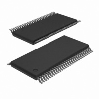
56-TSSOP
Lead Free Status / RoHS Status
Lead free / RoHS Compliant
Other names
74ALVCH16646DG-T
74ALVCH16646DG-T
935262421118
74ALVCH16646DG-T
935262421118


1. C
Philips Semiconductors
FEATURES
DESCRIPTION
The 74ALVCH16646 consists of 16 non-inverting bus transceiver
circuits with 3-State outputs, D-type flip-flops and control circuitry
arranged for multiplexed transmission of data directly from the
internal registers. Data on the ‘A’ or ‘B’ bus will be clocked in the
internal registers, as the appropriate clock (CP
HIGH logic level. Output enable (OE) and direction (DIR) inputs are
provided to control the transceiver function. In the transceiver mode,
data present at the high-impedance port may be stored in either the
‘A’ or ‘B’ register, or in both. The select source inputs (S
can multiplex stored and real-time (transparent mode) data. The
direction (DIR) input determines which bus will receive data when
OE is active (LOW). In the isolation mode (OE = HIGH), ‘A’ data
may be stored in the ‘B’ register and/or ‘B’ data may be stored in the
‘A’ register.
When an output function is disabled, the input function is still
enabled and may be used to store and transmit data. Only one of
the two buses, ‘A’ or ‘B’ may be driven at a time.
To ensure the high impedance state during power up or power
down, OE should be tied to V
QUICK REFERENCE DATA
GND = 0V; T
NOTES:
ORDERING INFORMATION
56-Pin Plastic TSSOP Type II
1998 Sep 03
Complies with JEDEC standard no. 8-1A
CMOS low power consumption
MULTIBYTE
Low inductance, multiple V
and ground bounce
Direct interface with TTL levels
Current drive
Output drive capability 50 transmission lines @ 85 C
All inputs have bushold circuitry
16-bit bus transceiver/register (3-State)
t
C
C
C
F
PHL
P
f
f
S (C
SYMBOL
i
o
max
I
PD
PD
D
= input frequency in MHz; C
= output frequency in MHz; V
= C
/t
L
PLH
is used to determine the dynamic power dissipation (P
PD
V
amb
PACKAGES
CC
TM
V
2
= 25 C; t
CC
24 mA at 3.0 V
flow-through pin-out architecture
Propagation delay
nAx to nBx
Input capacitance
Power dissipation capacitance per channel
Power dissipation capacitance per channel
Maximum clock frequency
f
2
o
) = sum of outputs.
f
i
+ S (C
r
= t
CC
CC
f
L
and ground pins for minimum noise
through a pullup resistor; the
2.5ns
L
PARAMETER
V
= output load capacity in pF;
CC
CC
= supply voltage in V;
2
TEMPERATURE RANGE
f
o
) where:
–40 C to +85 C
AB
or CP
BA
AB
) goes to a
and S
D
in W):
BA
V
V
V = GND to V
V
V
V
)
CC
CC
I
CC
CC
= GND to V
OUTSIDE NORTH AMERICA
= 2.5V, C
= 3.3V, C
= 2.5V, C
= 3.3V, C
2
74ALVCH16646 DGG
minimum value of the resistor is determined by the
current-sinking/current-sourcing capability of the driver.
Active bus-hold circuitry is provided to hold unused or floating data
inputs at a valid logic level.
PIN CONFIGURATION
L
L
L
L
CC
CC
= 30pF
= 50pF
= 30pF
= 50pF
1
1
CONDITIONS
Outputs enabled
Outputs disabled
1CP
2CP
1S
2S
1DIR
GND
GND
GND
GND
2DIR
V
V
1A0
1A1
1A2
1A3
1A4
1A5
1A6
1A7
2A0
2A1
2A2
2A3
2A5
2A6
2A4
2A7
CC
CC
AB
AB
AB
AB
NORTH AMERICA
7
10
11
12
13
14
15
16
17
18
19
20
21
22
23
24
25
26
27
28
1
2
3
4
5
6
8
9
ACH16646 DGG
74ALVCH16646
56
55
54
53
52
51
50
49
48
47
46
45
44
43
42
41
40
39
38
37
36
35
34
33
32
31
30
29
SY00011
1OE
1CP
1S
GND
1B0
1B1
V
1B2
1B3
1B4
GND
1B5
1B6
1B7
2B0
2B1
2B2
GND
2B3
2B4
2B5
V
2B6
2B7
GND
2S
2CP
2OE
CC
CC
BA
BA
TYPICAL
BA
BA
Product specification
300
320
2.6
2.7
3.0
36
4
DWG NUMBER
853-2116 19959
SOT364-1
UNIT
MHz
pF
pF
pF
ns
Related parts for 74ALVCH16646DGG:11
Image
Part Number
Description
Manufacturer
Datasheet
Request
R

Part Number:
Description:
NXP Semiconductors designed the LPC2420/2460 microcontroller around a 16-bit/32-bitARM7TDMI-S CPU core with real-time debug interfaces that include both JTAG andembedded trace
Manufacturer:
NXP Semiconductors
Datasheet:

Part Number:
Description:
NXP Semiconductors designed the LPC2458 microcontroller around a 16-bit/32-bitARM7TDMI-S CPU core with real-time debug interfaces that include both JTAG andembedded trace
Manufacturer:
NXP Semiconductors
Datasheet:
Part Number:
Description:
NXP Semiconductors designed the LPC2468 microcontroller around a 16-bit/32-bitARM7TDMI-S CPU core with real-time debug interfaces that include both JTAG andembedded trace
Manufacturer:
NXP Semiconductors
Datasheet:
Part Number:
Description:
NXP Semiconductors designed the LPC2470 microcontroller, powered by theARM7TDMI-S core, to be a highly integrated microcontroller for a wide range ofapplications that require advanced communications and high quality graphic displays
Manufacturer:
NXP Semiconductors
Datasheet:
Part Number:
Description:
NXP Semiconductors designed the LPC2478 microcontroller, powered by theARM7TDMI-S core, to be a highly integrated microcontroller for a wide range ofapplications that require advanced communications and high quality graphic displays
Manufacturer:
NXP Semiconductors
Datasheet:
Part Number:
Description:
The Philips Semiconductors XA (eXtended Architecture) family of 16-bit single-chip microcontrollers is powerful enough to easily handle the requirements of high performance embedded applications, yet inexpensive enough to compete in the market for hi
Manufacturer:
NXP Semiconductors
Datasheet:
Part Number:
Description:
The XA-S3 device is a member of Philips Semiconductors? XA(eXtended Architecture) family of high performance 16-bitsingle-chip microcontrollers
Manufacturer:
NXP Semiconductors
Datasheet:

Part Number:
Description:
The NXP BlueStreak LH75401/LH75411 family consists of two low-cost 16/32-bit System-on-Chip (SoC) devices
Manufacturer:
NXP Semiconductors
Datasheet:
Part Number:
Description:
The NXP LPC3130/3131 combine an 180 MHz ARM926EJ-S CPU core, high-speed USB2
Manufacturer:
NXP Semiconductors
Datasheet:
Part Number:
Description:
The NXP LPC3141 combine a 270 MHz ARM926EJ-S CPU core, High-speed USB 2
Manufacturer:
NXP Semiconductors
Part Number:
Description:
The NXP LPC3143 combine a 270 MHz ARM926EJ-S CPU core, High-speed USB 2
Manufacturer:
NXP Semiconductors

Part Number:
Description:
The NXP LPC3152 combines an 180 MHz ARM926EJ-S CPU core, High-speed USB 2
Manufacturer:
NXP Semiconductors
Part Number:
Description:
The NXP LPC3154 combines an 180 MHz ARM926EJ-S CPU core, High-speed USB 2
Manufacturer:
NXP Semiconductors

Part Number:
Description:
Standard level N-channel enhancement mode Field-Effect Transistor (FET) in a plastic package using NXP High-Performance Automotive (HPA) TrenchMOS technology
Manufacturer:
NXP Semiconductors
Datasheet: