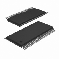
74ALVCH16823DGG:11 NXP Semiconductors, 74ALVCH16823DGG:11 Datasheet - Page 2

74ALVCH16823DGG:11
Manufacturer Part Number
74ALVCH16823DGG:11
Description
74ALVCH16823DGG/TSSOP56/TUBE-B
Manufacturer
NXP Semiconductors
Series
74ALVCHr
Type
D-Type Busr
Datasheet
1.74ALVCH16823DGG11.pdf
(12 pages)
Specifications of 74ALVCH16823DGG:11
Function
Master Reset
Output Type
Tri-State Non Inverted
Number Of Elements
2
Number Of Bits Per Element
9
Frequency - Clock
300MHz
Delay Time - Propagation
2.8ns
Trigger Type
Positive Edge
Current - Output High, Low
24mA, 24mA
Voltage - Supply
2.3 V ~ 2.7 V
Operating Temperature
-40°C ~ 85°C
Mounting Type
Surface Mount
Package / Case
56-TSSOP
Lead Free Status / RoHS Status
Lead free / RoHS Compliant
Other names
74ALVCH16823DG
74ALVCH16823DG
935259030112
74ALVCH16823DG
935259030112
1.
FEATURES
QUICK REFERENCE DATA
GND = 0V; T
NOTES:
ORDERING INFORMATION
Philips Semiconductors
56-Pin Plastic SSOP Type II
56-Pin Plastic TSSOP Type II
1998 Jul 29
Wide supply voltage range of 1.2V to 3.6V
Complies with JEDEC standard no. 8-1A.
CMOS low power consumption
Direct interface with TTL levels
Current drive
Multibyte flow-through standard pin-out architecture
Low inductance multiple V
ground bounce
All data inputs have bus hold
Output drive capability 50 transmission lines @ 85 C
18-bit D-type flip-flop (3-State)
t
F
C
C
C
PHL
SYMBOL
max
I
PD
C
P
f
f
S (C
i
o
D
PD
= input frequency in MHz; C
/t
= output frequency in MHz; V
PLH
= C
L
is used to determine the dynamic power dissipation (P
PD
amb
PACKAGES
V
CC
= 25 C; t
V
2
24 mA at 3.0 V
Propagation delay
CP to Qn
Maximum clock frequency
Input capacitance
Power dissipation capacitance per latch
Power dissipation capacitance per latch
CC
f
2
o
) = sum of outputs.
f
i
r
+ S (C
= t
CC
f
and GND pins to minimize noise and
2.5ns
L
PARAMETER
L
= output load capacity in pF;
V
CC
CC
TEMPERATURE RANGE
= supply voltage in V;
2
f
o
-40 C to +85 C
-40 C to +85 C
) where:
D
V
V
V
V
V = GND to V
V
in mW):
CC
CC
CC
CC
I
OUTSIDE NORTH AMERICA
= GND to V
= 2.5V, CL = 30pF
= 3.3V, CL = 50pF
= 2.5V, CL = 30pF
= 3.3V, CL = 50pF
2
74ALVCH16823 DGG
74ALVCH16823 DL
DESCRIPTION
The 74ALVCH16823 is a 18-bit edge-triggered flip-flop featuring
separate D-type inputs for each flip-flop and 3-state outputs for bus
oriented applications. Incorporates bushold data inputs which
eliminate the need for external pull-up resistors to hold unused
inputs. The74ALVCH16823 consists of two sections of nine
edge-triggered flip-flops. A clock (CP) input, an output-enable (OE)
input, a Master reset (MR) input and a clock-enable( CE) input are
provided for each total 9-bit section.
With the clock-enable (CE) input LOW, the D-type flip-flops will store
the state of their individual D-inputs that meet the set-up and hold
time requirements on the LOW-to-HIGH CP transition. Taking CE
HIGH disables the clock buffer, thus latching the outputs. Taking the
Master reset (MR) input LOW causes all the Q outputs to go LOW
independently of the clock.
When OE is LOW, the contents of the flip-flops are available at the
outputs. When the OE is HIGH, the outputs go to the high
impedance OFF-state. Operation of the OE input does not affect the
state of flip-flops.
Active bus hold circuitry is provided to hold unused or floating data
inputs at a valid logic level.
CC
CC
1
1
CONDITIONS
Outputs disabled
Outputs enabled
NORTH AMERICA
ACH16823 DGG
ACH16823 DL
74ALVCH16823
TYPICAL
Product specification
300
350
2.1
2.1
5.0
16
10
DWG NUMBER
853–2100 19800
SOT371-1
SOT364-1
UNIT
MHz
ns
pF
pF
pF


