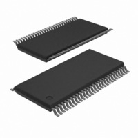
74AVCM162836DGG:11 NXP Semiconductors, 74AVCM162836DGG:11 Datasheet - Page 6

74AVCM162836DGG:11
Manufacturer Part Number
74AVCM162836DGG:11
Description
74AVCM162836DGG/TSSOP56/REEL13
Manufacturer
NXP Semiconductors
Series
74AVCMr
Datasheet
1.74AVCM162836DGG11.pdf
(10 pages)
Specifications of 74AVCM162836DGG:11
Logic Type
Buffer/Line Driver, Non-Inverting
Number Of Elements
1
Number Of Bits Per Element
20
Current - Output High, Low
12mA, 12mA
Voltage - Supply
1.2 V ~ 3.6 V
Operating Temperature
-40°C ~ 85°C
Mounting Type
Surface Mount
Package / Case
56-TSSOP
Lead Free Status / RoHS Status
Lead free / RoHS Compliant
Other names
74AVCM162836DG-T
74AVCM162836DG-T
935264252118
74AVCM162836DG-T
935264252118
1. All typical values are measured at T
Philips Semiconductors
AC CHARACTERISTICS
GND = 0 V; t
NOTES:
AC WAVEFORMS FOR V
V
V
V
V
output load.
V
AC WAVEFORMS FOR V
V
V
V
V
V
output load.
V
2001 Apr 20
SYMBOL
t
t
t
M
X
Y
OL
I
M
X
Y
OL
I
PHL
CC
PZH
PHZ
= V
= V
20-bit registered driver with inverted register enable
and 15
F
= V
= V
= V
= V
Waveform 1. Input (An) to output (Yn) propagation delay
= 0.5 V
= 0.5 V
t
t
t
and V
and V
max
SU
t
W
V
A
INPUT
GND
V
Y
OUTPUT
V
/t
/t
/t
h
< 2.3 V RANGE
CC
CC
I
n
OH
n
OL
PLH
OL
OH
OL
OH
PZL
PLZ
+ 0.300 V
+ 0.15 V
– 0.300 V
– 0.15 V
OH
OH
CC
CC
NOTE: V
r
Maximum clock pulse frequency
Propagation delay An to Yn
Propagation delay LE to Yn
Propagation delay CP to Yn
3-State output enable time OE
to Yn
3-State output disable time OE
to Yn
CP pulse width HIGH or LOW
LE pulse width HIGH
Set-up time An to CP
Set-up time An to LE HIGH
Set-up time An to LE LOW
Hold time An to CP
Hold time An to LE HIGH
Hold time An to LE LOW
are the typical output voltage drop that occur with the
are the typical output voltage drop that occur with the
= t
f
M
2.0 ns; C
V
termination resistors (3-State)
= 0.5V
M
t
PARAMETER
PHL
CC
at V
L
= 30 pF
V
M
CC
CC
CC
= 2.3 to 2.7 V
= 3.0 V TO 3.6 V RANGE
= 2.3 V TO 2.7 V AND
amb
= 25 C and at V
WAVE-
FORM
FORM
t
PLH
1, 7
2, 7
3, 7
6, 7
6, 7
3, 7
2, 7
5, 7
4, 7
4, 7
5, 7
4, 7
4, 7
3, 7
MIN
SH00132
500
0.7
0.7
0.7
1.0
1.0
1.0
1.0
0.7
0.5
0.5
0.9
1.6
1.4
V
CC
CC
= 3.3
= 1.8 V, 2.5 V, 3.3 V.
TYP
1.7
2.0
1.9
2.5
2.5
–
–
–
–
–
–
–
–
–
1
0.3 V
MAX
6
2.5
2.7
2.5
4.5
3.5
–
–
–
–
–
–
–
–
–
Waveform 2. Latch enable input (LE) pulse width, the latch
MIN
400
Yn OUTPUT
0.8
0.8
0.8
1.0
1.0
1.2
1.2
0.7
0.5
0.5
0.9
1.7
1.5
V
CC
LE INPUT
enable input to output (Yn) propagation delays.
= 2.5
GND
V
V
TYP
OH
OL
2.0
2.4
2.2
2.8
2.4
V
–
–
–
–
–
–
–
–
–
I
NOTE: V
1
LIMITS
0.2 V
MAX
3.1
3.3
3.0
4.5
4.0
–
–
–
–
–
–
–
–
–
M
= 0.5 V
V
t
PHL
M
MIN
V
250
1.0
1.0
1.0
1.5
1.5
2.0
2.0
0.7
0.5
0.6
1.0
2.0
1.7
CC
t
CC
W
at V
= 1.8
TYP
V
2.6
3.0
2.8
3.5
4.0
M
CC
–
–
–
–
–
–
–
–
–
= 2.3 to 2.7 V
1
74AVCM162836
0.15 V
MAX
4.5
5.0
4.5
6.5
6.5
–
–
–
–
–
–
–
–
–
t
PLH
V
M
V
MIN
Product specification
1.0
0.2
2.0
1.5
3.2
2.8
CC
–
–
–
–
–
–
–
–
SH00165
= 1.2 V
TYP
5.2
5.6
5.2
5.5
6.9
–
–
–
–
–
–
–
–
–
UNIT
MHz
ns
ns
ns
ns
ns
ns
ns
ns
ns
ns
ns


