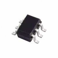
AD5601BKSZ-REEL7 Analog Devices Inc, AD5601BKSZ-REEL7 Datasheet - Page 4

AD5601BKSZ-REEL7
Manufacturer Part Number
AD5601BKSZ-REEL7
Description
IC,D/A CONVERTER,SINGLE,8-BIT,CMOS,TSSOP,6PIN
Manufacturer
Analog Devices Inc
Series
nanoDAC™r
Datasheet
1.AD5601BKSZ-REEL7.pdf
(20 pages)
Specifications of AD5601BKSZ-REEL7
Settling Time
6µs
Number Of Bits
8
Data Interface
Serial
Number Of Converters
1
Voltage Supply Source
Single Supply
Power Dissipation (max)
500µW
Operating Temperature
-40°C ~ 125°C
Mounting Type
Surface Mount
Package / Case
SC-70-6, SC-88, SOT-363
Number Of Channels
1
Resolution
8b
Conversion Rate
1.7MSPS
Interface Type
Serial (3-Wire, SPI, QSPI, Microwire)
Single Supply Voltage (typ)
3.3/5V
Dual Supply Voltage (typ)
Not RequiredV
Architecture
Resistor-String
Power Supply Requirement
Single
Output Type
Voltage
Integral Nonlinearity Error
±0.5LSB
Single Supply Voltage (min)
2.7V
Single Supply Voltage (max)
5.5V
Dual Supply Voltage (min)
Not RequiredV
Dual Supply Voltage (max)
Not RequiredV
Operating Temp Range
-40C to 125C
Operating Temperature Classification
Automotive
Mounting
Surface Mount
Pin Count
6
Package Type
SC-70
Lead Free Status / RoHS Status
Lead free / RoHS Compliant
Lead Free Status / RoHS Status
Lead free / RoHS Compliant
Other names
AD5601BKSZ-REEL7
AD5601BKSZ-REEL7TR
AD5601BKSZ-REEL7TR
Available stocks
Company
Part Number
Manufacturer
Quantity
Price
Company:
Part Number:
AD5601BKSZ-REEL7
Manufacturer:
STM
Quantity:
2 853
Part Number:
AD5601BKSZ-REEL7
Manufacturer:
ADI/亚德诺
Quantity:
20 000
AD5601/AD5611/AD5621
Parameter
POWER REQUIREMENTS
POWER EFFICIENCY
1
2
3
TIMING CHARACTERISTICS
V
Table 3.
Parameter
t
t
t
t
t
t
t
t
t
1
2
1
2
3
4
5
6
7
8
9
Linearity calculated using a reduced code range: AD5621 from Code 64 to Code 4032; AD5611 from Code 16 to Code 1008; AD5601 from Code 4 to Code 252.
Guaranteed by design and characterization, not production tested.
Total current flowing into all pins.
All input signals are specified with tr = tf = 1 ns/V (10% to 90% of V
Maximum SCLK frequency is 30 MHz.
DD
2
V
I
I
I
DD
DD
OUT
DD
= 2.7 V to 5.5 V; all specifications T
V
V
V
V
for Normal Mode
/I
for All Power-Down Modes
DD
DD
DD
DD
DD
= ±4.5 V to ±5.5 V
= ±2.7 V to ±3.6 V
= ±4.5 V to ±5.5 V
= ±2.7 V to ±3.6 V
SYNC
SCLK
SDIN
Limit
33
5
5
10
5
4.5
0
20
13
1
t
8
t
4
Min
2.7
D15
MIN
Unit
ns min
ns min
ns min
ns min
ns min
ns min
ns min
ns min
ns min
to T
Typ
75
60
0.5
0.2
96
A Grade
D14
MAX
t
3
, unless otherwise noted. See Figure 2.
t
2
Max
5.5
100
90
DD
) and timed from a voltage level of (V
Figure 2. Timing Diagram
Test Conditions/Comments
SCLK cycle time
SCLK high time
SCLK low time
SYNC to SCLK falling edge setup time
Data setup time
Data hold time
SCLK falling edge to SYNC rising edge
Minimum SYNC high time
SYNC rising edge to next SCLK falling edge ignored
t
1
Rev. E | Page 4 of 20
D2
Min
2.7
t
5
Typ
75
60
0.5
0.2
96
B Grade
D1
t
6
D0
Max
5.5
100
90
t
7
IL
t
9
+ V
IH
Unit
V
μA
μA
μA
μA
%
)/2.
Test Conditions/Comments
All digital inputs at 0 V or V
DAC active and excluding load
current
V
V
V
V
V
I
LOAD
D15
IH
IH
IH
IH
IH
= V
= V
= V
= V
= V
= 2 mA and V
DD
DD
DD
DD
DD
and V
and V
and V
and V
and V
D14
IL
IL
IL
IL
IL
= GND
= GND
= GND
= GND
= GND
DD
= ±5 V
DD


