a
PRODUCT DESCRIPTION
The AD75004 contains four complete, voltage output, 12-bit
digital-to-analog converters, a high stability bandgap reference,
and double-buffered input latches on a single chip. The convert-
ers use 12 precision high speed bipolar current steering switches
and laser-trimmed thin-film resistor networks to provide fast
settling time and high accuracy.
Microprocessor compatibility is achieved by the on-chip
double-buffered latches. The design of the input latches allows
direct interface to 8-bit buses. The 12 bits of data from the first
rank of latches can then be transferred to the second rank,
avoiding generation of spurious analog output values. The latch
responds to strobe pulses as short as 50 ns, allowing use with
fast microprocessors.
The functional completeness and high performance of the
AD75004 results from a combination of advanced switch de-
sign, the BiMOS II fabrication process, and proven laser trim-
ming technology. BiMOS II is an epitaxial BiCMOS process
optimized for analog and converter functions. The AD75004 is
trimmed at the wafer level and is specified to 1/2 LSB maxi-
mum linearity error at 25 C and 3/4 LSB over the full operat-
ing temperature range. The on-chip output amplifiers provide
an output range of 5 V, with 1 LSB equal to 2.44 mV.
REV. A
Information furnished by Analog Devices is believed to be accurate and
reliable. However, no responsibility is assumed by Analog Devices for its
use, nor for any infringements of patents or other rights of third parties
which may result from its use. No license is granted by implication or
otherwise under any patent or patent rights of Analog Devices.
FEATURES
4 Complete 12-Bit D/A Functions
Double-Buffered Latches
Simultaneous Update of All DACs Possible
High Stability Bandgap Reference
Monolithic BiMOS Construction
Guaranteed Monotonic over Temperature
3/4 LSB Linearity Guaranteed over Temperature
4 s max Settling Time to 0.01%
Operates with
Low Power: 720 mW max Including Reference
TTL/5 V CMOS Compatible Logic Inputs
8-Bit Microprocessor Interface
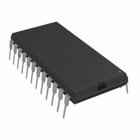
24-Pin PDIP or 28-Lead PLCC Package
5 V Output Range
12 V Supplies
The bandgap reference on the chip has low noise, long term
stability and temperature drift characteristics comparable to
discrete reference diodes. The absolute value of the reference is
laser trimmed to +5.00 V with 0.6% maximum error. Its tem-
perature coefficient is also laser trimmed.
Typical full-scale gain TC is 15 ppm/ C. With guaranteed
One Technology Way, P.O. Box 9106, Norwood, MA 02062-9106, U.S.A.
Tel: 617/329-4700
monotonicity over the full temperature range, the AD75004 is
well suited for wide temperature range performance.
D7
D6
D5
D4
D3
D2
D1
D0
REFERENCE
+5V
INPUTS
VOLTAGE
8-BIT
V
BUS
TTL
REFOUT
FUNCTIONAL BLOCK DIAGRAM
LATCHES
LATCHES
LATCHES
LATCHES
LATCHES
8 + 4-BIT
8 + 4-BIT
8 + 4-BIT
8 + 4-BIT
CS WR
INPUT
CONTROL LOGIC
V
TTL INPUTS
REFIN
2.22k
A3 A2 A1 A0
LATCHES
LATCH
LATCH
LATCH
LATCH
12-BIT
12-BIT
12-BIT
12-BIT
DAC
D/A Converter
12-BIT
12-BIT
12-BIT
12-BIT
DAC
DAC
DAC
DAC
AD75004
Quad 12-Bit
AD75004
Fax: 617/326-8703
10k
10k
10k
10k
+12V
–12V
V
V
V
V
V
DGND
V
AGND
OUT1
OUT0
SS
OUT3
OUT2
DD


