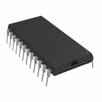
AD75004KNZ Analog Devices Inc, AD75004KNZ Datasheet - Page 3

AD75004KNZ
Manufacturer Part Number
AD75004KNZ
Description
QUAD 12-BIT DAC, PDIP IC
Manufacturer
Analog Devices Inc
Datasheet
1.AD75004KNZ.pdf
(4 pages)
Specifications of AD75004KNZ
Settling Time
4µs
Number Of Bits
12
Data Interface
Parallel
Number Of Converters
4
Voltage Supply Source
Dual ±
Power Dissipation (max)
720mW
Operating Temperature
0°C ~ 70°C
Mounting Type
Through Hole
Package / Case
24-DIP (0.600", 15.24mm)
Lead Free Status / RoHS Status
Lead free / RoHS Compliant
REV. A
TIMING CHARACTERISTICS
(T
Parameter
Address Setup Time
Address Hold Time
Data Setup Time
Data Hold Time
Chip Select to Write Setup Time
Write to Chip Select Hold Time
Write Pulse Width
NOTES
1
Specifications subject to change without notice
CAUTION
ESD (electrostatic discharge) sensitive device. Electrostatic charges as high as 4000 V readily
accumulate on the human body and test equipment and can discharge without detection.
Although the AD75004 features proprietary ESD protection circuitry, permanent damage may
occur on devices subjected to high energy electrostatic discharges. Therefore, proper ESD
precautions are recommended to avoid performance degradation or loss of functionality.
Model
AD75004KN
AD75004KP
*N = Plastic DIP; P = Plastic Leaded Chip Carrier.
Timing measurement reference level is 1.5 V.
A
ADDRESS INPUTS
= +25 C,
(A0–A3)
DATA INPUTS
CHIP SELECT
(D0–D7)
(CS)
WRITE
(WR)
12.0 V power supplies unless otherwise noted)
*Stresses above those listed under “Absolute Maximum Ratings” may cause permanent damage to the device. These are stress
ABSOLUTE MAXIMUM RATINGS*
(T
V
V
V
V
Digital Inputs to DGND
AGND to DGND
Short to AGND on Analog Outputs
Power Dissipation
Specification Temperature Range
Storage Temperature
Lead Temperature
Temperature Range
0 C to +70 C
0 C to +70 C
ratings only and functional operation of the device at these or any other conditions above those indicated in the operational
sections of this specification is not implied. Exposure to absolute maximum rating conditions for extended periods may affect
device reliability.
DD
SS
DD
REFIN
A
ORDERING GUIDE
= +25 C unless otherwise noted)
to DGND
to DGND
to V
to AGND
SS
t
1
t
5
Symbol
t
t
t
t
t
t
t
1
2
3
4
5
6
7
t
7
1
t
3
Package Option*
N-24A
P-28A
t
t
2
4
Min
30
10
10
45
0
0
50
t
6
Units
ns
ns
ns
ns
ns
ns
ns
Min
–0.3
–18
–0.3
–0.3
–0.3
–0.3
0
–65
–3–
Control and Address Lines
CS
1
X
0
0
0
0
NOTE
*The A1 and A0 inputs specify the relevant channel.
Max
+18
+0.3
+26.4
V
V
+0.3
1.0
+70
Indefinite
+150
+300
DD
DD
A1
0
0
1
1
WR A3
X
1
0
0
0
0
A0
0
1
0
1
X
X
0
0
1
1
Units
V
V
V
V
V
V
sec
W
C
C
C
Channel
0
1
2
3
A2
X
X
0
1
0
1
Conditions
T
Soldering, 10 seconds
TRUTH TABLE
A1
X
X
A1* A0*
A1* A0*
A1* A0*
X
A
75 C
A0
X
X
X
WARNING!
Operation
No operation
No operation
8 LSBs
4 MSBs
Update one DAC latch
Update all 4 DAC latches
ESD SENSITIVE DEVICE
AD75004
one input latch
one input latch


